Plasma display panel, and apparatus and method for driving the same
a technology of display panel and plasma, which is applied in the direction of gas discharge electrodes, instruments, and address electrodes, etc., can solve the problems of increasing the switching loss when it is turned, the actual switch ssub>c /sub>is not capable of zero-voltage switching, and the inability to perform zero-voltage switching of the switch constituting the circuit, etc., to reduce the rising/falling time of the panel voltage, the effect of reducing the inrush curren
- Summary
- Abstract
- Description
- Claims
- Application Information
AI Technical Summary
Benefits of technology
Problems solved by technology
Method used
Image
Examples
first embodiment
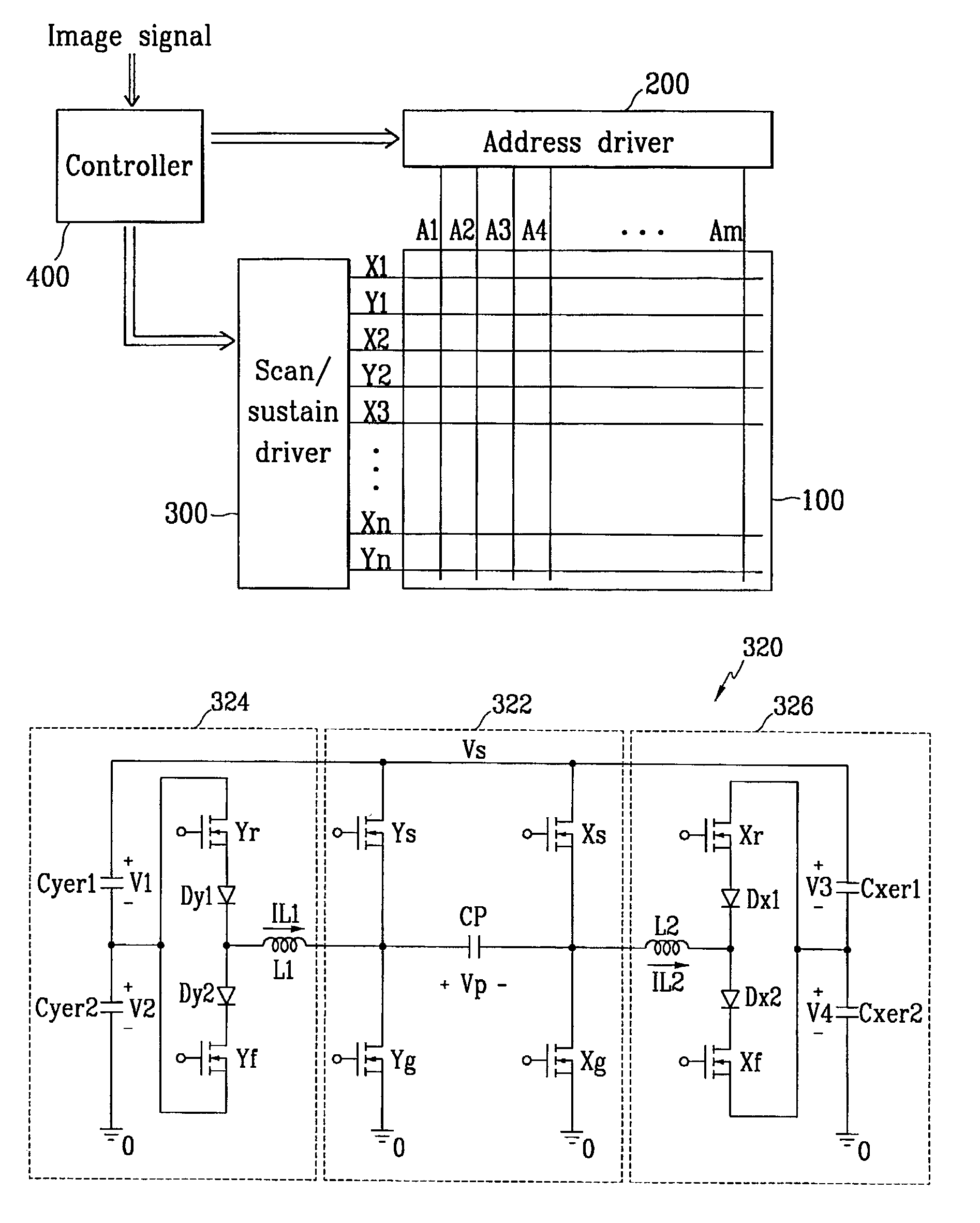
[0063]The scan / sustain driver 300 according to the embodiment of the present invention includes an energy recovery circuit for recovering a reactive power and reusing it. FIG. 6 illustrates an energy recovery circuit 320 in accordance with the present invention.
[0064]As illustrated in FIG. 6, the energy recovery circuit 320 according to the embodiment of the present invention comprises a sustain discharge unit 322, a Y electrode charge / discharge unit 324, and an X electrode charge / discharge unit 326.
[0065]The sustain discharge unit 322 comprises four sustain switches Ys, Yg, Xs and Xg, each of which is composed of a MOSFET that has a body diode connected to a sustain discharge voltage VS or a ground voltage. The switching operations of these four switches allow the terminal voltages Vy and Vx of panel capacitor CP to be maintained at the sustain discharge voltage VS or the ground voltage.
[0066]The Y electrode charge / discharge unit 324 comprises energy recovery capacitors Cyer1 and C...
second embodiment
[0097]When the interval where the gate signals of the energy recovery switches Yr and Xr overlap those of the sustain switches Ys, Yg, Xs and Xg is longer than the interval where the gate signals of the energy recovery switches Yf and Xf overlap those of the sustain switches Ys, Yg, Xs and Xg, as shown in FIG. 10 according to the present invention, the discharging current of the capacitors Cyer2 and Cxer2 becomes higher than their charging current, as shown in FIG. 11. Accordingly, the terminal voltages V2 and V4 of the respective capacitors Cyer2 and Cxer2 are below VS / 2.
third embodiment
[0098]To the contrary, when the interval where the gate signals of the energy recovery switches Yr and Xr overlap those of the sustain switches Ys, Yg, Xs and Xg is shorter than the interval where the gate signals of the energy recovery switches Yf and Xf overlap those of the sustain switches Ys, Yg, Xs and Xg, as shown in FIG. 12 according to the present invention, the discharging current of the capacitors Cyer2 and Cxer2 becomes lower than the charging current of them, as shown in FIG. 13. Accordingly, the terminal voltages V2 and V4 of the respective capacitors Cyer2 and Cxer2 are above VS / 2.
[0099]The driving timing diagrams shown in FIGS. 10 and 12 respectively according to the second embodiment and the third embodiment of the present invention use the same circuit as the energy recovery circuit shown in FIG. 6. However, the driving timing of the switches is different. The operation of the energy recovery circuit according to the second embodiment and the third embodiment of the...
PUM
 Abstract
Description
Claims
Application Information
 - R&D
- Intellectual Property
- Life Sciences
- Materials
- Tech Scout
- Unparalleled Data Quality
- Higher Quality Content
- 60% Fewer Hallucinations
Browse by: Latest US Patents, China's latest patents, Technical Efficacy Thesaurus, Application Domain, Technology Topic, Popular Technical Reports.
© 2025 PatSnap. All rights reserved.Legal|Privacy policy|Modern Slavery Act Transparency Statement|Sitemap|About US| Contact US: help@patsnap.com


