Display unit

a display device and display technology, applied in the field of display devices, can solve the problems of large drive power, large mass, slow response, etc., and achieve the effects of high brightness display devices, low power consumption, and high reliability

Inactive Publication Date: 2006-04-04
JAPAN SCI & TECH CORP
View PDF24 Cites 11 Cited by
  • Summary
  • Abstract
  • Description
  • Claims
  • Application Information

AI Technical Summary

Benefits of technology

[0038]As explained above, the inventions of this application effectively scatter the guided light through changes in form such as by opaquing, deformation, and coloring, by guiding the light through the optical waveguide comprising the pair of the first optical wave guide and the second waveguide, also through the second optical waveguide generally containing transparent electroresponsive materials, and by applying the image signal voltage across the pair electrodes sandwiching the electroresponsive materials. Thus, the inventions offer low power consuming and high brightness display devices. The inventions of this application can use a transparent plate as the clad portion of the optical waveguide and also can use it as the supporting board.
[0039]The optical waveguide can be arranged and formed on one side of the plate. Thus, the optical wave guide does not need mechanical strength, allows a number of thin and fine optical waveguides to be arrayed in high density, and has no mechanical displacement portion, enabling it to offer small-to-large display devices of high reliability and fine high quality pixel. Also, because the core of the optical waveguide is not exposed, no foreign matter such as dust or dirt will adhere to the optical waveguide portion of the optical waveguide. Thus, the display devices of the inventions of this application can provide optimal performance even in inferior environments. The main materials of the image display for the display device such as transparent plates, optical waveguide, and clad portion can be made of plastic, which can be flexibly bent mechanically, thus making it possible to offer light-weight and impact-resistant display devices. Also, because the pixels emit scattered light, the inventions can offer display devices with a wide viewing angle, different from conventional devices that use a back light, and liquid crystal combined with the polarizer as an optical shutter. Also, the display devices of the inventions are capable of not only monochromic display, but also two-color or full-color display by guiding the light of two colors or three primary colors through the corresponding waveguide (100). The display devices transmit the light from light sources such as light-emitting diodes (LED) and laser diodes (LD) of three primary colors, red (R), green (G), and blue (B) to the pixel portion through thin optical waveguides. Further, as they require no polarizer or color filter, the devices can directly emit scattered light to the outside and can be made thin. Thus, the display devices of this invention are bright compact and cost-effective. Also, the full-color display devices have independent optical waveguides of three primary colors, red (R), green (G), and blue (B), so that the respective waveguides can display pixels made of independent cells for the three primary colors only. Although they use a sequential drive system, the display devices can be adjusted so that, even when the next pixel portion is selected, the preceding pixel portion can emit light at the same time. Thus, the display devices are bright, with extremely little flickering.
[0040]Also, the display devices have the advantage of low power consumption, because they can use not only the internal light source, but also an external light source. Also, the pair of the first optical waveguide and the second optical waveguide that comprise the optical wave guide, and the pair of the electrode and its wiring that form a matrix-like pixel, can be joined or located closely to each other by forming one of the pair on a plate and the other on a different plate. Thus, the devices can be assembled using good parts only, thereby raising the yield of non-defective components and lowering the prices of the displays accordingly.
[0041]Further, the optical waveguide is divided into the pair of the first optical waveguide and the second optical waveguide that comprise the waveguide, thereby making the first optical waveguide sufficiently transparent and bright against the guided light and allowing part of the light guided through the first optical waveguide to be coupled and propagated to the second optical waveguide. Thus, this display device is suitable for a large screen even when the second optical waveguide is not very transparent against the guided light because the guided light is sufficiently propagated to the first optical waveguide.
[0042]The first optical waveguide is a multi-mode waveguide to guide a large amount of light, and the light is guided at various angles. When the second optical waveguide has a lower refractive index than that of the first optical waveguide, part of the light propagating through the first optical waveguide at a large angle leaks to become the light propagated through second optical waveguide.
[0043]When the second optical waveguide has a higher refractive index than that of the first optical waveguide, and a layer with a lower refractive index is formed between the first optical waveguide and the second refractive waveguide (The layer may be an air gap of proximity, liquid crystal alignment film, or other transparent layer), the second optical waveguide acts as having an equivalent lower refractive index. Thus, the second optical waveguide is equivalent to an optical waveguide that has a lower refractive index than the above first optical waveguide.

Problems solved by technology

However, a problem with the conventional displacement transmission unit driven by a piezoelectric actuator was the thick piezoelectric element needed to transmit a large displacement, resulting in large mass, requiring large drive power, and producing slow response.
The system with the reflection prism, an electrostatic extraction unit, located close to the optical waveguide has a problem in that its reflection prism has to have a large mass and is unable to provide high-speed response.
Further, the electrodes to drive the extraction unit by static electricity are almost parallel to each other and are located at a distance through a support, thus requiring large voltage for attraction.
Also, the optical switch to leak the guided light by attracting the cantilever thin film to the optical waveguide by static electricity has a problem in that it needs high voltage for attraction because the cantilever film is isolated from the optical waveguide.
Additionally, the system that uses light leakage through the contact part of the above-mentioned optical waveguide and drive unit has its problems.
It is unreliable due to fatigue of its mechanical drive unit, has unexpected scattering of the guided light due to foreign matter such as dust sticking to the core of the optical waveguide which is exposed to the air, and its contact part must be a thick and heavy drive unit to ensure large leakage of the guided light and pixels with sufficient brightness.
It is difficult to see clearly: it varies greatly depending on the viewing angle because the system emits the light from the back light through the liquid crystal and uses a polarizer.
Further, it is difficult to produce in thin configurations because it has a complex structure comprising a color filter and polarizer, and thus has is also expensive.
First, because its optical waveguide is exposed, foreign matter such as dust sticks to its surface, causing the guided light to leak and degrade the quality of the image second, the two glass plates, which are used also as the optical waveguide, are the supporting materials and have to be thick. Thus, it is difficult to form a thin and precise optical waveguide.
Third, instead of miniaturizing the optical waveguide, the light of the three primary colors is guided through the same optical waveguide, and each pixel is set to scattering mode synchronously with the light emission, so that the light of the three primary colors can use the liquid crystal pixel of one point for full-color display. This system needs only one third of the pixels that the conventional method needs. But, brightness is necessary to see an image. The shining of one pixel for an instant is too dark. Flickering is large unless the sequentially driven pixels emit light simultaneously. Thus, it is difficult to get a screen of high brightness with such a system because it uses only a transient residual image.
Fourth, comprising two glass plates, the board is too hard to provide a flexible image display of the screen and is vulnerable to impact and damage.
The display device that scatters the light from the initially provided light output unit by changing the refractive index at the light output control unit provided in the optical waveguide and by guiding the guided light to the light control unit cannot provide a screen of the required brightness.
This is because currently available liquid crystals cannot produce sufficient changes in the refractive index for only a pixel of about 100 É m to guide enough light to the light output control unit.

Method used


Image

  • Display unit
  • Display unit
  • Display unit

Examples


embodiment 1

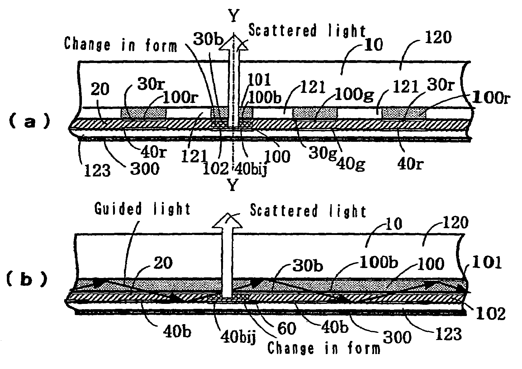
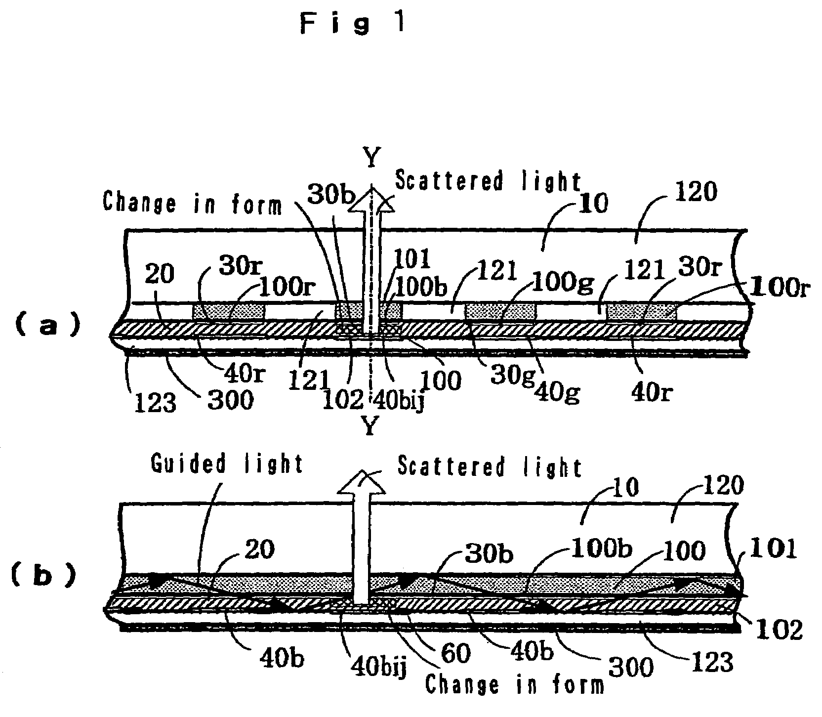
[0059]FIG. 1 illustrates an embodiment of the component of the display device of this invention using dynamic scattering liquid crystal as the electroresponsive material 20, and transparent plate 10 as the clad portion 120 of the optical waveguide 100 comprising the pair of the first optical waveguide 101 and the second optical waveguide 102. The component also uses the plate 10 as the supporting board for the thin optical waveguide 100. In addition, the three primary colors, optical waveguide for the color red 100r, optical waveguide for the color green 100g, and optical waveguide for the color blue 100b, are arrayed sequentially on both sides of the transparent clad portion 121, so that the device is capable of full-color display.

[0060]FIG. 1 also illustrates how the electroresponsive material 20 becomes murky and causes the blue light, or the guided light, to be emitted outside the transparent plate 10 and observed as a blue pixel. The electroresponsive material 20 comprises the ...

embodiment 2

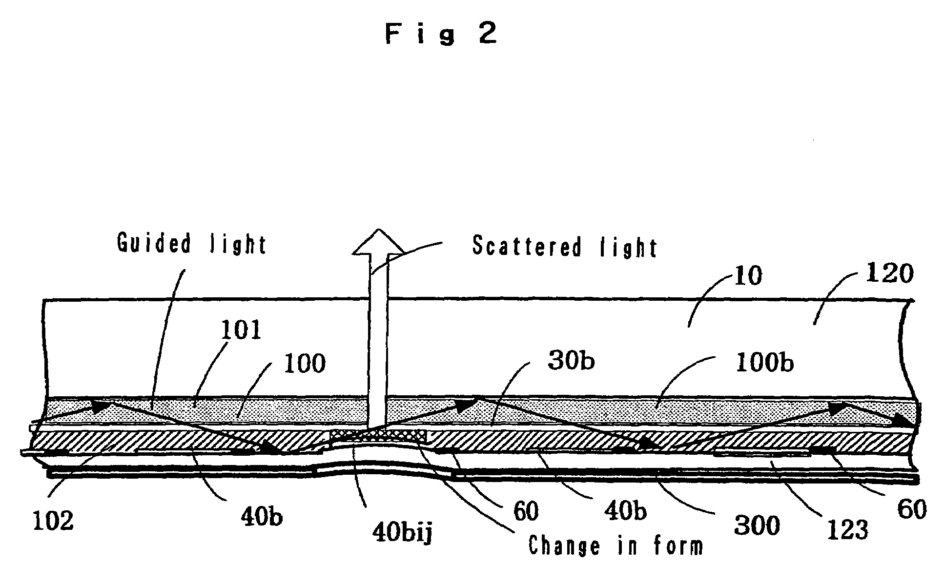
[0067]FIG. 2 shows the longitudinal sectional views along the optical waveguide 100b for the color blue, using a jelly-like gel (electroresponsive gel) that expands and shrinks under an electric field as the electroresponsive material 20 for the display device of this invention, as is shown in FIG. 1(b). When a color image signal voltage is applied between the transparent electrode 30b and the electrode 40ij selected from the electrode 40, paired to the electrode 30b, the electroresponsive gel that will become the second optical waveguide 102 changes in form (shrinks), decreasing its sectional area. Thus, the blue light guided there is scattered and emitted outside the transparent plate 10. Gel used as artificial muscle is suitable for the electroresponsive gel. Transparent polyurethane gel, for example, can also be used. Epoxy sheet or polyethylene sheet of about 50 É m thickness that deforms easily according to the expansion and shrinkage of the gel can be used as the clad portion...

embodiment 3

[0068]Differing from FIG. 1 in Embodiment 1, FIG. 3 shows the horizontal sectional views of an embodiment in which only several optical waveguides 100r for the color red and 100b for the color blue are formed sandwiching the clad portions 121 on the same plane of the plate 10, while the optical waveguide 100g for the color green is formed periodically on the clad portion 123 sandwiched by the clad portion 122. Each optical waveguide 100g for the color green is located between the optical waveguides 100r for the color red and 100b for the color blue. Also in FIG. 3, the image signal voltage over the threshold limit value is applied to the pair electrodes comprising the transparent electrode 30b and the electrode 40bij formed on the optical waveguide 100b for the color blue. The electric field thus caused makes the electroresponsive material 20 (Light-scattering liquid crystal layer of the second optical waveguide 102) murky and emits the scattered light to the outside as pixels from ...


PUM

PropertyMeasurementUnit
voltageaaaaaaaaaa
refractive indexaaaaaaaaaa
transparentaaaaaaaaaa

Abstract

A display unit comprising a board (10), a three-primary color-independent optical waveguide (100) arranged and formed on one side thereof, and a transparent electrode (30) and an electrode (40) serving as counter electrodes arranged and formed to sandwich an electric field reaction material (20) formed on one of two optical waveguides constituting the optical waveguide (100) and being transparent to waveguide light, wherein part of the waveguide light is allowed to pass at least the field reaction material (20), and a voltage applied between these counter electrodes changes the shape of the reaction material (20) to scatter the waveguide light and form pixels in to a displayed image, whereby the device is free from a mechanical drive unit, high in reliability, quality, brightness and response speed, low in power consumption and cost, and capable of full color displaying.

Description

TECHNICAL FIELD[0001]This invention relates to a display device featuring very bright, thin and small-to-large screens, low power consumption and high-speed response. It relates especially to a display device that produces an image by scattering guided light by diffusing, expanding, shrinking, deforming, or coloring transparent electroresponsive material contained between paired electrodes by applying a voltage between the electrodes at points corresponding to specific pixels.BACKGROUND OF THE INVENTION[0002]Conventional thin display devices display images by adjusting the light leaking from the optical waveguide by controlling the contact and separation of the displacement transmission unit with and from the optical waveguide using a piezoelectric actuator (see Japanese Laid-Open Patent Publication Nos. H7-287176, H10-78549 and H11-73142). Also, there are conventionally proposed systems that leaked evanescent waves by bringing a reflection prism, an extraction unit driven by static...

Claims


Application Information

Patent Timeline
Patent Type & Authority Patents(United States)
IPC IPC(8): G02B6/00G02B26/08G02F1/1333G02F1/13357G02F1/137G02F1/1524G02F1/157G09F9/35G09F9/37
CPCG02F1/133621G02F1/195G02F1/1375G02F1/19G02F1/1523G02F1/1524
Inventor KIMURA
Owner JAPAN SCI & TECH CORP
Why Eureka
Try Eureka