
LSI package

a technology of large-scale integration and packaging, applied in the direction of printed circuits, semiconductor devices, semiconductor/solid-state device details, etc., can solve the problems of not being supplied with a sufficiently high voltage at the power supply terminal of the lsi chip, too large voltage drop in the single-source voltage supply terminal to be ignored, etc., to reduce unnecessary electromagnetic radiation from the lsi package, reduce noise from outside, and suppress unnecessary electromagnetic radiation

Inactive Publication Date: 2006-03-21
PANASONIC CORP
View PDF3 Cites 8 Cited by
  • Summary
  • Abstract
  • Description
  • Claims
  • Application Information

AI Technical Summary

Benefits of technology

[0024]According to an LSI package having the above-mentioned construction, high-frequency currents generated by a switching operation in an internal circuit in an LSI chip flow into power supply terminals on an LSI chip. However, the high-frequency currents flow into earth through a capacitor element. In addition, since the voltage at the capacitor element is applied to the power supply terminals on the LSI chip, the voltage at the power supply terminals does not fall. Similarly, since the high-frequency currents do not flow into source voltage supply terminals on the LSI package, the voltage at the source voltage supply terminals does not fall either. As a result, a steady voltage is supplied with the power supply terminals on the LSI chip. Thus, the number of source voltage supply terminals on the LSI package can be reduced so as to be smaller than the number of power supply terminals on the LSI chip. Accordingly, a pitch of terminals as a whole (including signal terminals) on the LSI package is more or less increased. As a result, board manufacturing can be made easier without increasing the size of the surface of the LSI package on which terminals are to be provided.
[0025]Also, since the capacitor element is directly connected to the terminals on the LSI chip, a path for the high-frequency currents can be made remarkably short. This effectively suppresses unnecessary electromagnetic radiation.
[0027]Since an inductance element is provided, unnecessary electromagnetic radiation can be suppressed more effectively, and noise from outside can be prevented.
[0028]Since a conductive board is provided and essential elements such as the LSI chip are enclosed by vias, unnecessary electromagnetic radiation from the LSI package can be reduced and radiation noise from outside can be prevented.

Problems solved by technology

However, when a switching operation occurs in circuits connected to the power supply terminals on the LSI chip, high-frequency currents are generated, and flow into the single source voltage supply terminal on the LSI package.
This causes too large a voltage fall in a voltage at the single source voltage supply terminal to be ignored.
Consequently, the power supply terminals on the LSI chip are not supplied with a sufficiently high voltage.

Method used


Image

  • LSI package
  • LSI package
  • LSI package

Examples


Embodiment Construction

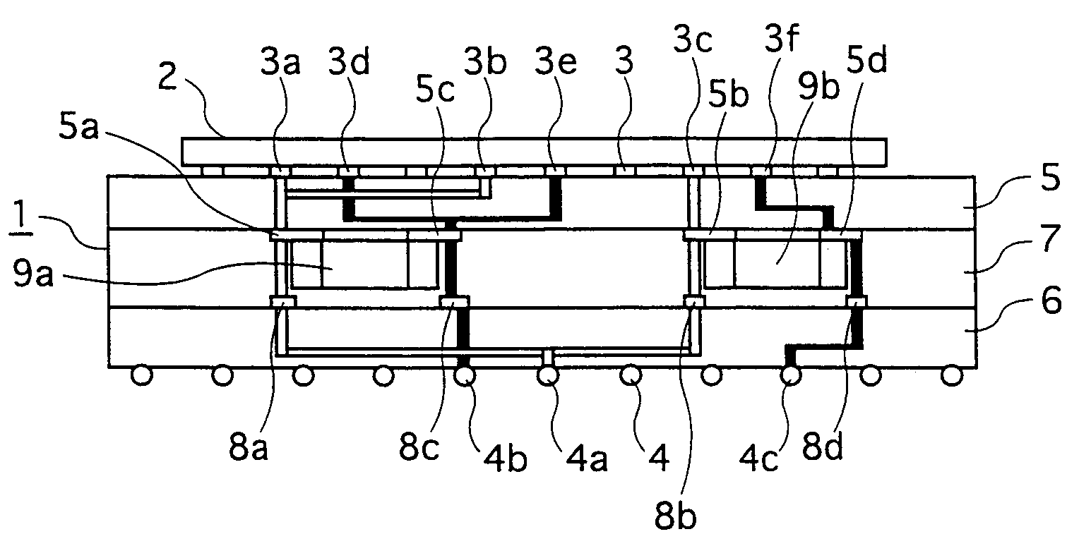
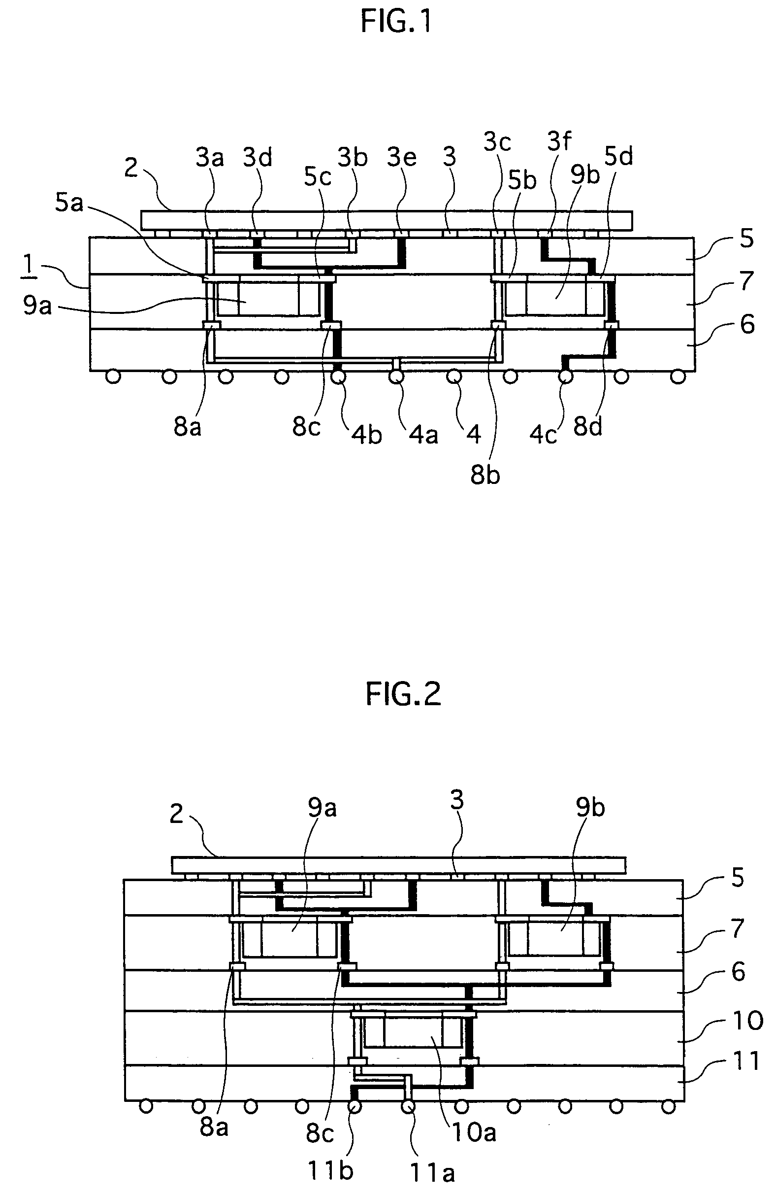
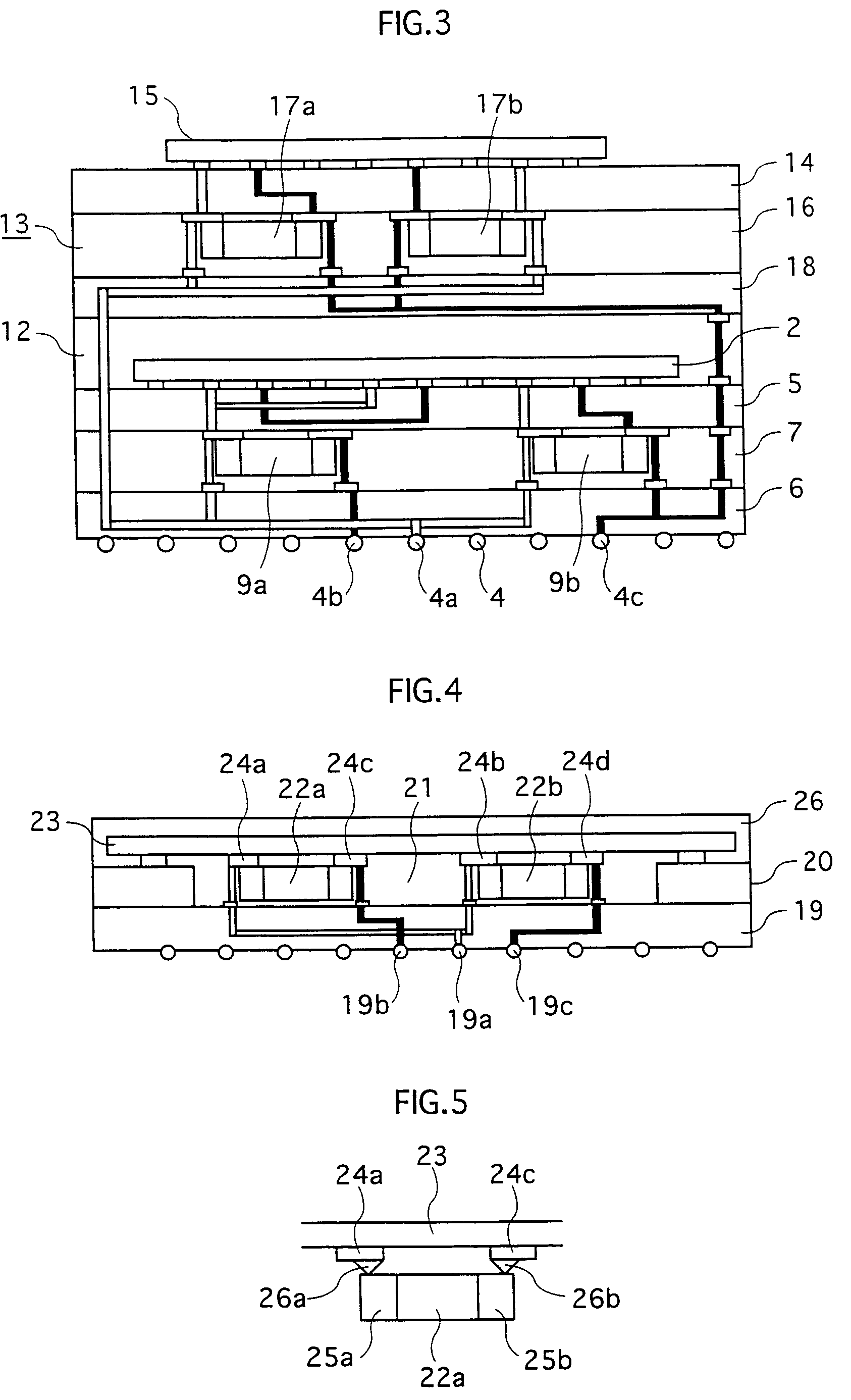
[0042]The following part describes LSI packages relating to embodiments of the present invention with reference to the attached figures. The attached figures show the cross sections of the LSI packages, and do not include hatchings for better understanding of the construction.

[0043]As shown in FIG. 1, an LSI package is constituted by a substrate 1 forming the main body of the LSI package and an LSI chip 2. A plurality of bumps are arranged in a grid pattern, as terminals 3, on the LSI chip 2. A plurality of solder balls are arranged in a grid pattern, as terminals 4, on one surface of the substrate 1. The terminals 3 and 4 include signal input / output terminals, power supply terminals, and earth terminals. Signal input / output terminals are not directly related to the present invention, and therefore not explained here.

[0044]The substrate 1 has a three-layer construction, which includes a multilayer circuit board 6 on which the terminals 4 are provided, a multilayer circuit board 5 on...


PUM


Abstract

According to LSI packages of the BGA type and the like, the number of source voltage supply terminals on an LSI package needs to be around the same as the number of power supply terminals on an LSI chip, in order to prevent the impact of high-frequency currents generated due to a switching operation in an internal circuit in the LSI chip. According to the present invention, however, at least two power supply terminals on an LSI chip are connected to one source voltage supply terminal on an LSI package. In addition, a capacitor element is embedded in a substrate forming the main body of the LSI package, and the capacitor element is provided between a source voltage supply terminal and an earth terminal.

Description

BACKGROUND OF THE INVENTION[0001](1) Field of the Invention[0002]The present invention relates to an Large Scale Integration (LSI) packaging technology.[0003](2) Prior Art[0004]The number of pins in an LSI has been recently on the rise in accordance with a demand for more sophisticated LSIs. On the other hand, a miniaturized package is desired for LSIs in accordance with a demand for miniaturized devices and boards. For this reason, Ball Grid Array (BGA) types shown in FIG. 9A and FIG. 9B and Chip Size Packages (CSPs) have replaced Quad Flat Packages (QFPs) shown in FIG. 8A and FIG. 8B. According to CSP types, the size of an LSI package is substantially the same as that of an LSI chip. According to BGA and CSP LSI packaging technologies, terminals (solder balls) to be connected to the wiring of printed-wiring boards are arranged in a grid pattern on a back surface of an LSI package.[0005]In LSI packages of BGA and CSP, solder balls located near the periphery can be connected, by wir...

Claims


Application Information

Patent Timeline
Patent Type & Authority Patents(United States)
IPC IPC(8): H01L23/52H01L23/48H01L25/00H01L23/498H01L23/50H01L23/538H05K1/18
CPCH01L23/49822H01L23/50H01L23/5389H01L2224/16225H01L2924/3025H05K1/185H01L2924/15311H01L2224/05573H01L2224/05568H01L2924/00014H01L2224/05599
Inventor SUENAGA, HIROSHISAITO, YOSHIYUKI
Owner PANASONIC CORP
Learn More