
Communication semiconductor integrated circuit with frequency adjustment/control circuit

a technology of frequency adjustment and control circuit, which is applied in the direction of pulse automatic control, angular modulation details, electrical apparatus, etc., can solve the problems of inability to adjust the modulation-based frequency displacement variation amount, and the frequency displacement amount varies, so as to achieve the effect of reducing the circuit scal

Inactive Publication Date: 2006-03-14
RENESAS TECH CORP
View PDF7 Cites 24 Cited by
  • Summary
  • Abstract
  • Description
  • Claims
  • Application Information

AI Technical Summary

Benefits of technology

[0017]According to the present invention, since the shift in the amount of frequency displacement can be corrected by the frequency adjustment means, the amount of modulation-based frequency displacement of the voltage-controlled oscillator circuit can be adjusted in a state in which the communication semiconductor integrated circuit having the voltage-controlled oscillator circuit has been packaged on a system. It is thus possible to correct a variation in the amount of modulation-based frequency displacement of the voltage-controlled oscillator circuit without trimming in the manufacturing process and correct even a shift in the amount of frequency displacement due to a change in operating environment.
[0018]Preferably, the frequency adjustment means is configured so as to be capable of generating a signal corresponding to the difference between a measurement value of the frequency of the voltage-controlled oscillator circuit and a target value and changing the value of each of capacitors constituting the voltage-controlled oscillator circuit in accordance with the signal, thereby adjusting even the carrier frequency of a carrier. Thus, both the carrier frequency of the oscillation output of the voltage-controlled oscillator circuit and the amount of modulation-based frequency displacement can be corrected by the common circuit, and hence a circuit scale can be reduced as compared with the case in which discrete adjustment means are provided.

Problems solved by technology

The frequency modulation system has a problem in that the amount of displacement of the frequency varies even it is modulated with the same transmit data in addition to a variation in carrier frequency.
Therefore, the modulating voltage-controlled oscillator employed in a transmission system of a wireless communication system in which modulation information is given to the voltage-controlled oscillator has a problem in that it cannot reach up to an adjustment to the variation in the amount of modulation-based frequency displacement.

Method used


Image

  • Communication semiconductor integrated circuit with frequency adjustment/control circuit
  • Communication semiconductor integrated circuit with frequency adjustment/control circuit
  • Communication semiconductor integrated circuit with frequency adjustment/control circuit

Examples


Embodiment Construction

[0029]Preferred embodiments of the present invention will hereinafter be described with reference to the accompanying drawings.

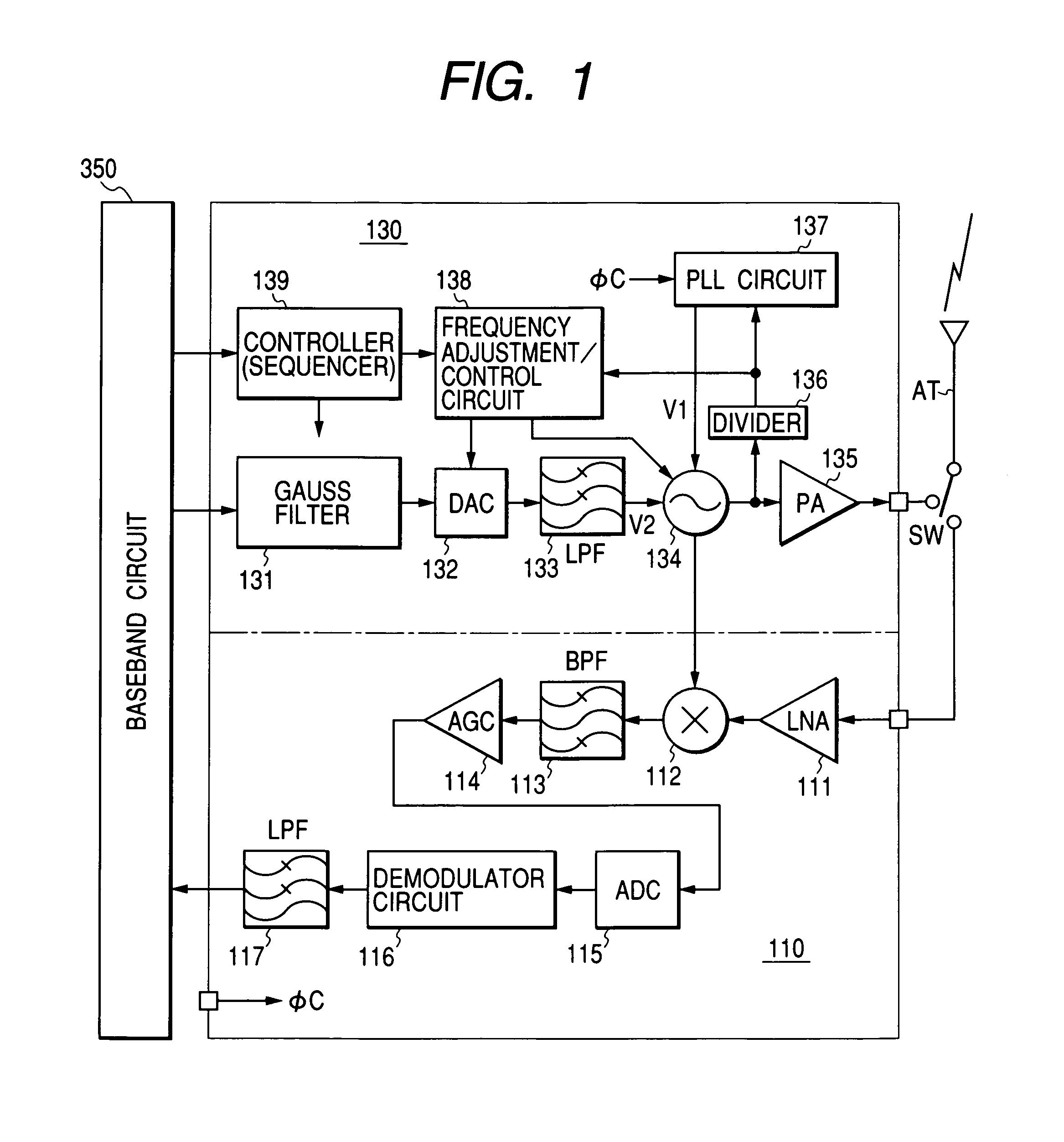
[0030]A configurational example of a wireless communication system suitable for application of a communication semiconductor integrated circuit according to the present invention is shown in FIG. 1.

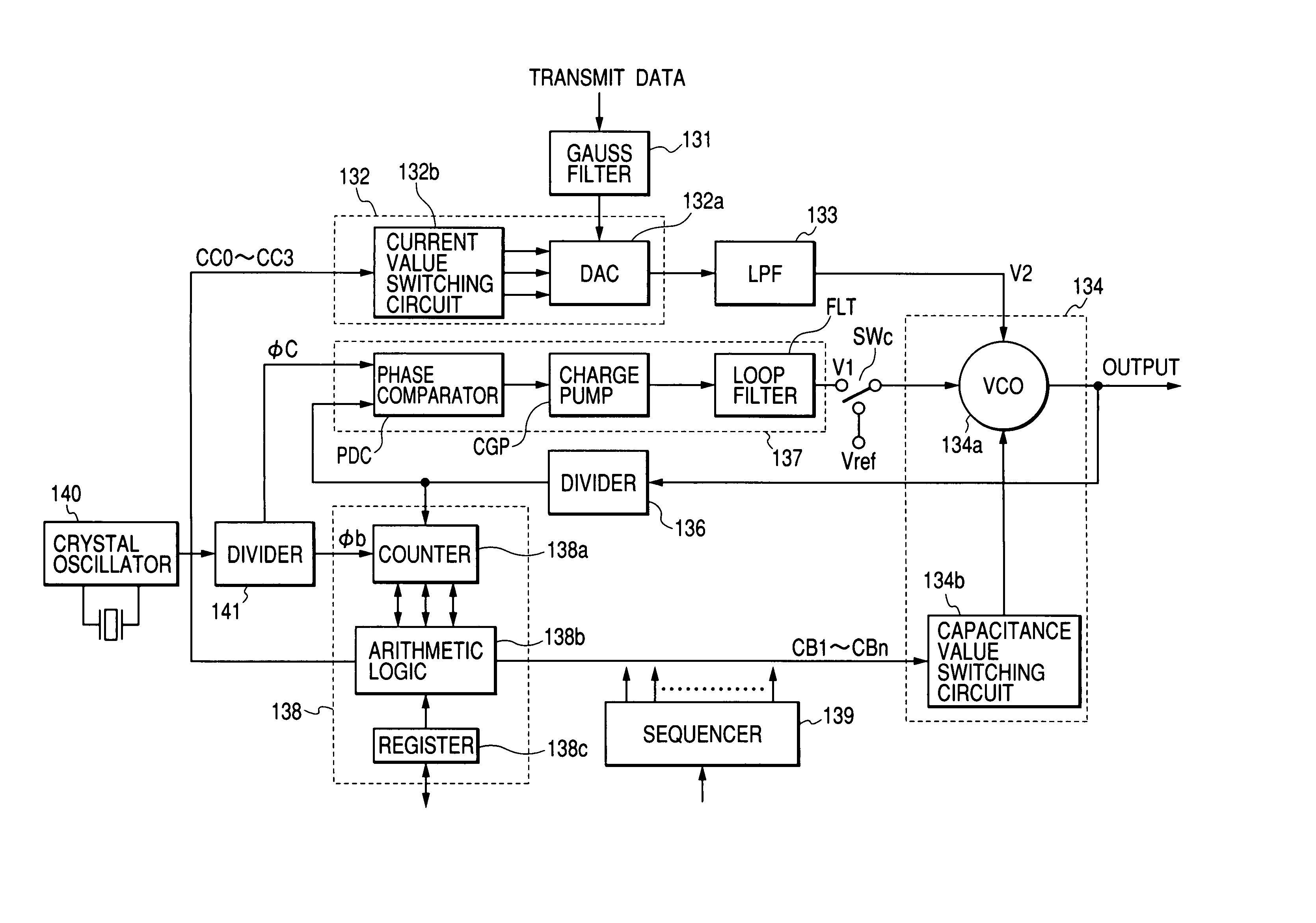
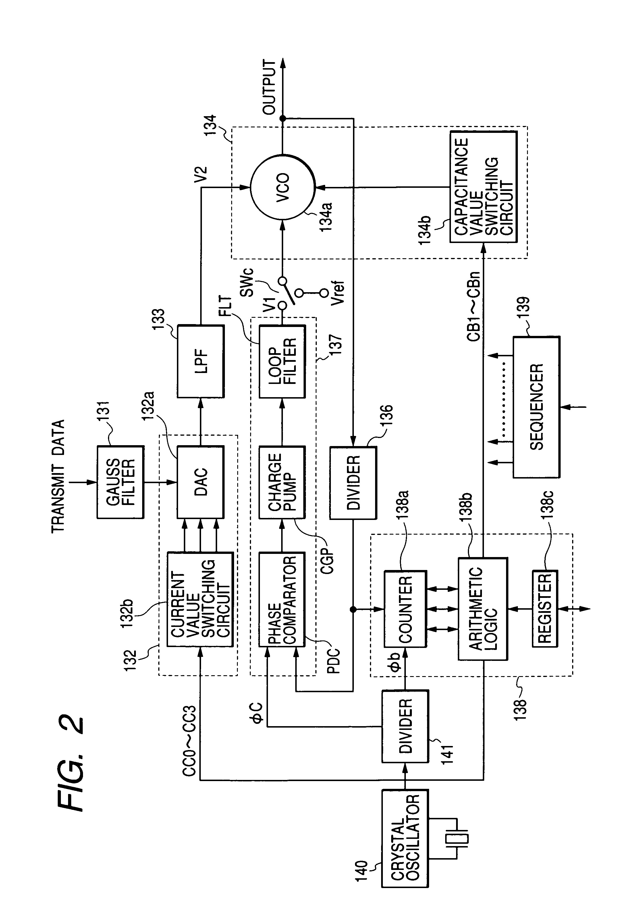
[0031]In FIG. 1, AT indicates an antenna which transmits and receives a signal wave, SW indicates a transmit-receive changeover switch, reference numeral 110 indicates a reception-system circuit which down-converts a signal received by the antenna AT to an intermediate frequency, demodulates and amplifies the same and converts the so-processed signal to a baseband signal, and reference numeral 130 indicates a transmission-system circuit which generates a carrier frequency signal, modulates the carrier frequency signal in accordance with a baseband signal outputted from a baseband circuit 350 and transmits the modulated signal via the antenna AT. The reception-syst...


PUM


Abstract

The present invention provides a communication semiconductor integrated circuit wherein a first control voltage for a voltage-controlled oscillator circuit is controlled based on a feedback signal sent from a PLL loop to generate a carrier frequency signal used as a carrier, and under the generation of the carrier frequency signal, a second control voltage for the voltage-controlled oscillator circuit is controlled based on the output of a DA converter circuit for DA-converting a code generated based on transmit data to thereby frequency-modulate an oscillation signal. The communication semiconductor integrated circuit is provided with a frequency adjustment / control circuit which measures the frequency of an oscillation output of the voltage-controlled oscillator circuit and adjusts a reference current value of the DA converter circuit according to the difference between the measured value and a target value to thereby correct the frequency.

Description

CROSS-REFERENCE TO RELATED APPLICATION[0001]The present application claims priority from Japanese patent application JP 2003-081734 filed on Mar. 25, 2003, the content of which is hereby incorporated by reference into this application.BACKGROUND OF THE INVENTION[0002]The present invention relates to a technique for adjusting an oscillation frequency of a voltage-controlled oscillator (VCO), and to, for example, a technique effective for application to a communication semiconductor integrated circuit employed in a transmission system of a wireless communication system, wherein a voltage-controlled oscillator is controlled based on transmit data while generating a carrier frequency signal (carrier) by the voltage-controlled oscillator to thereby frequency-modulate the carrier.[0003]In the standard called “Bluetooth” that sets the rules related to the transmission of data between peripheral devices such as a personal computer, a printer, etc. by wireless communication, a frequency modu...

Claims


Application Information

Patent Timeline
Patent Type & Authority Patents(United States)
IPC IPC(8): H03L7/197H03C3/09H03L7/089H03L7/099H03L7/10H03L7/14H03L7/18
CPCH03C3/0958H03L7/14H03L7/10H03L7/099H03L7/0891H03L7/104H03C3/0991
Inventor SUZUKI, JUNMIYAGAWA, HIROKAZUEZUMI, YOSHIYUKI
Owner RENESAS TECH CORP
Learn More