Gap forming pattern fracturing method for forming optical proximity corrected masking layer

a technology of optical proximity and masking layer, applied in the field of lithographic methods, to achieve the effect of convenient commercial implementation and convenient commercial implementation

Inactive Publication Date: 2006-03-14
TAIWAN SEMICON MFG CO LTD
View PDF7 Cites 4 Cited by
  • Summary
  • Abstract
  • Description
  • Claims
  • Application Information

AI Technical Summary

Benefits of technology

[0014]A second object of the present invention is to provide a charged particle beam method in accord with the first object of the present invention wherein there is attenuated a proximity effect when exposing the blanket resist layer while employing the charged particle beam method.
[0015]A third object of the present invention is to provide a method in accord with the first object of the invention and the second object of the invention, wherein the method is readily commercially implemented.
[0019]The present invention is readily commercially implemented. The present invention employs methods and materials as are generally known in the art of microelectronic fabrication, but employed within the context of particular design limitations and particular process limitations which provide at least in part the present invention. Since it is at least in part particular design limitations and particular process limitations which provide at least in part the present invention, rather than the existence of methods and materials which provides the present invention, the method of the present invention is readily commercially implemented.

Problems solved by technology

While direct lithographic writing methods, such as in particular direct electron beam lithographic writing methods, are thus desirable within the art of microelectronic fabrication for forming patterned resist layers which are employed either directly or indirectly for forming patterned microelectronic layers within microelectronic fabrications, direct lithographic writing methods, and in particular direct electron beam lithographic writing methods, are nonetheless not entirely without problems in the art of microelectronic fabrication for forming patterned resist layers which are employed either directly or indirectly for forming patterned microelectronic layers within microelectronic fabrications.

Method used


Image

  • Gap forming pattern fracturing method for forming optical proximity corrected masking layer
  • Gap forming pattern fracturing method for forming optical proximity corrected masking layer
  • Gap forming pattern fracturing method for forming optical proximity corrected masking layer

Examples


example

[0055]There was provided two photomask blanks each formed of a transparent quartz substrate of thickness about 0.76 centimeters, in turn having formed thereupon a blanket chromium layer of thickness about 700 angstroms. In turn, each of the blanket chromium layers had formed thereupon a blanket photoresist layer formed of a conventional electron beam photosensitive photoresist material formed to a thickness of about 4000 angstroms.

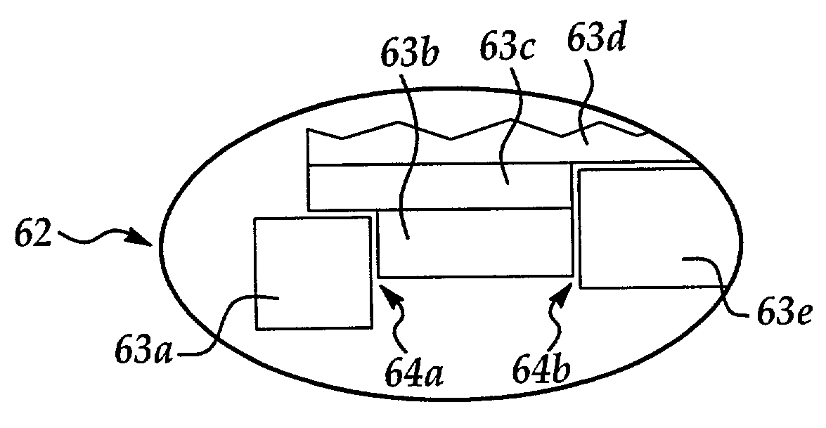
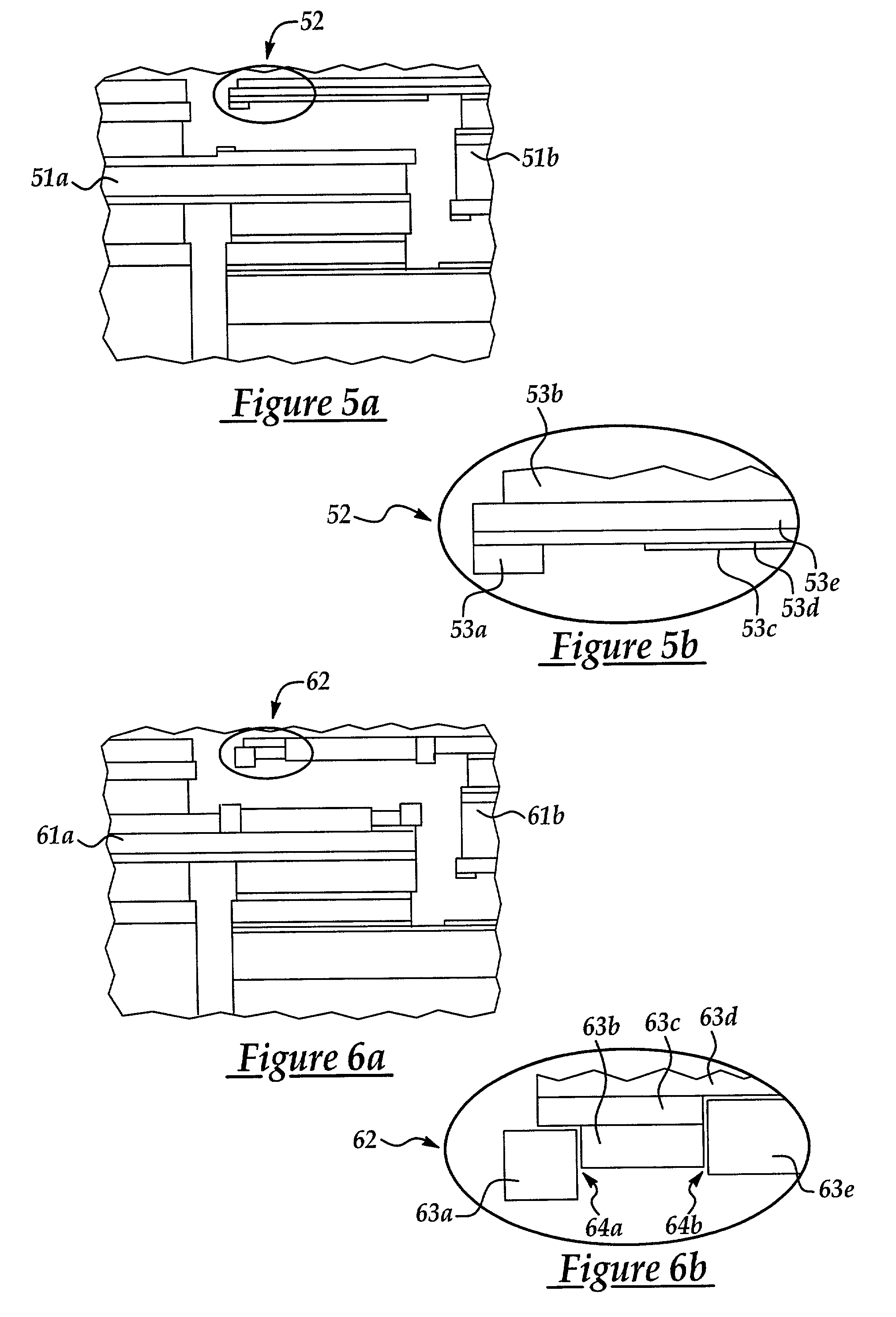
[0056]One of each of the two photomask blanks was then electron beam photoexposed in accord with either: (1) the electron beam pattern fracture map whose schematic plan view diagram is illustrated in FIG. 5a and FIG. 5b; or (2) the electron beam pattern fracture map whose schematic plan view diagram is illustrated in FIG. 6a and FIG. 6b. Within the photomask blank which was electron beam exposed in accord with the pattern fracture map whose schematic plan view diagram is illustrated in FIG. 6a and FIG. 6b, there was employed a series of gaps of linewidth a...


PUM

PropertyMeasurementUnit
widthaaaaaaaaaa
lengthaaaaaaaaaa
gap widthaaaaaaaaaa

Abstract

Within a charged particle beam exposure method for forming a patterned resist layer there is employed separating at least one adjacent pair of fractured pattern elements employed in forming a contiguous latent pattern within a blanket resist layer a gap. By employing the gap, a patterned resist layer formed incident to development of the blanket resist layer is formed with enhanced pattern fidelity and enhanced critical dimension control.

Description

BACKGROUND OF THE INVENTION[0001]1. Field of the Invention[0002]The present invention relates generally to lithographic methods employed for fabricating microelectronic fabrications. More particularly, the present invention relates to charged particle beam lithographic methods employed for fabricating microelectronic fabrications.[0003]2. Description of the Related Art[0004]Microelectronic fabrications are formed from microelectronic substrates over which are formed patterned microelectronic conductor layers which are separated by microelectronic dielectric layers. In the process of forming patterned microelectronic conductor layers within microelectronic fabrications, as well as in the process of forming other types of patterned microelectronic layers within microelectronic fabrications, further as well as in the process of forming patterned masking layers within photomasks which may be employed for forming patterned microelectronic layers of various varieties within microelectroni...

Claims


Application Information

Patent Timeline
Patent Type & Authority Patents(United States)
IPC IPC(8): G03F9/00G03C5/00G03F1/00G03F7/20
CPCG03F1/144G03F7/2059H01J2237/31769G03F1/78
Inventor HSIEH, REN-GUEY
Owner TAIWAN SEMICON MFG CO LTD
Why Eureka
Try Eureka