Material for contact etch layer to enhance device performance
a contact etch layer and material technology, applied in the field of thin films, can solve the problems of not being able to provide the conventional film and method of producing nitride liners and other films have not necessarily provided all the characteristics that may be desirable for field effect transistors (fets) and other applications, so as to achieve better conformity and load
- Summary
- Abstract
- Description
- Claims
- Application Information
AI Technical Summary
Benefits of technology
Problems solved by technology
Method used
Image
Examples
##ventive example 1
INVENTIVE EXAMPLE 1
[0069]A film (i.e., a nitride film) was deposited by reacting BTBAS and NH3 in a single wafer reactor. A process condition is selected which gives a carbon concentration of 3 to 15 atomic %.
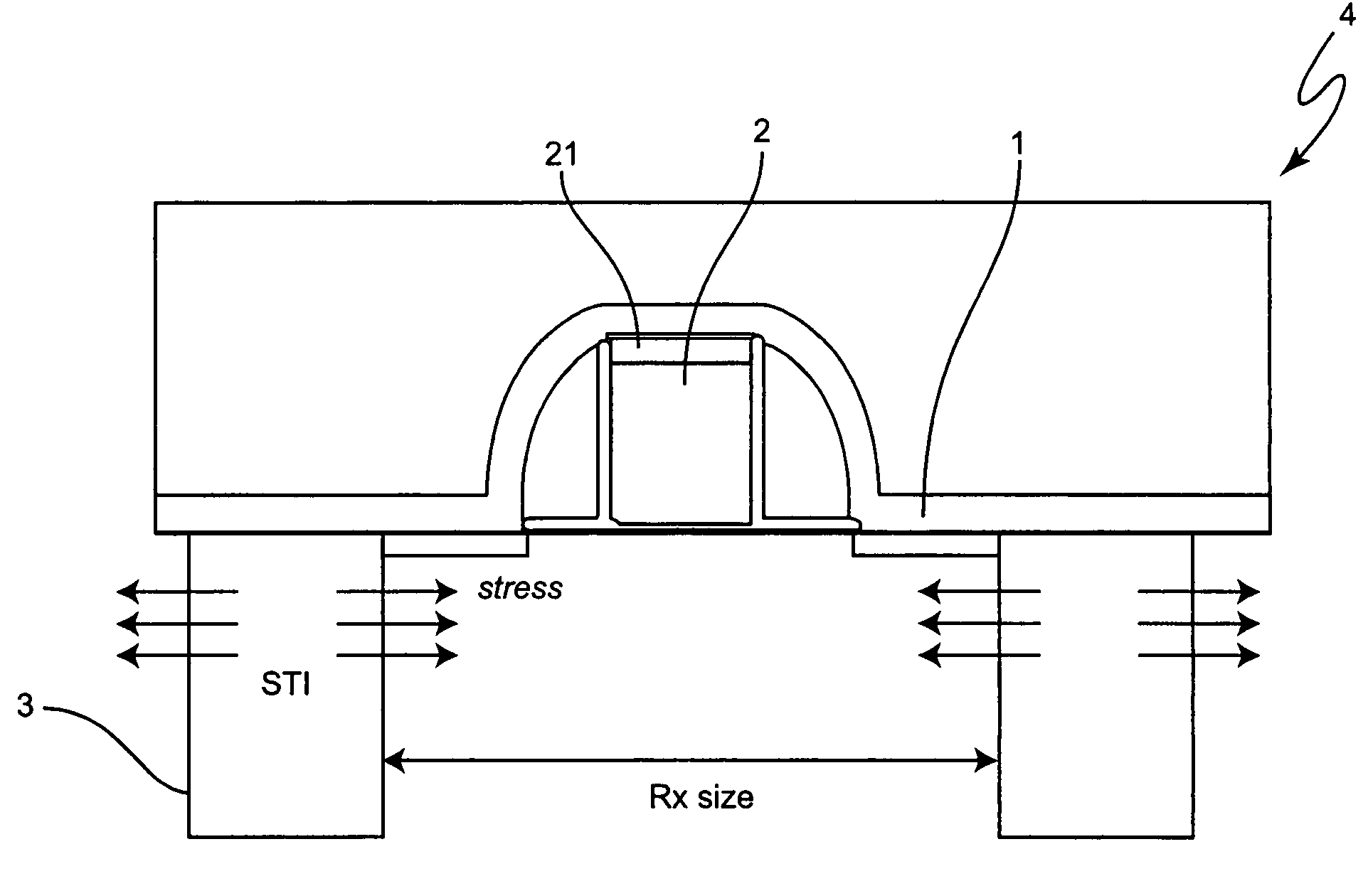
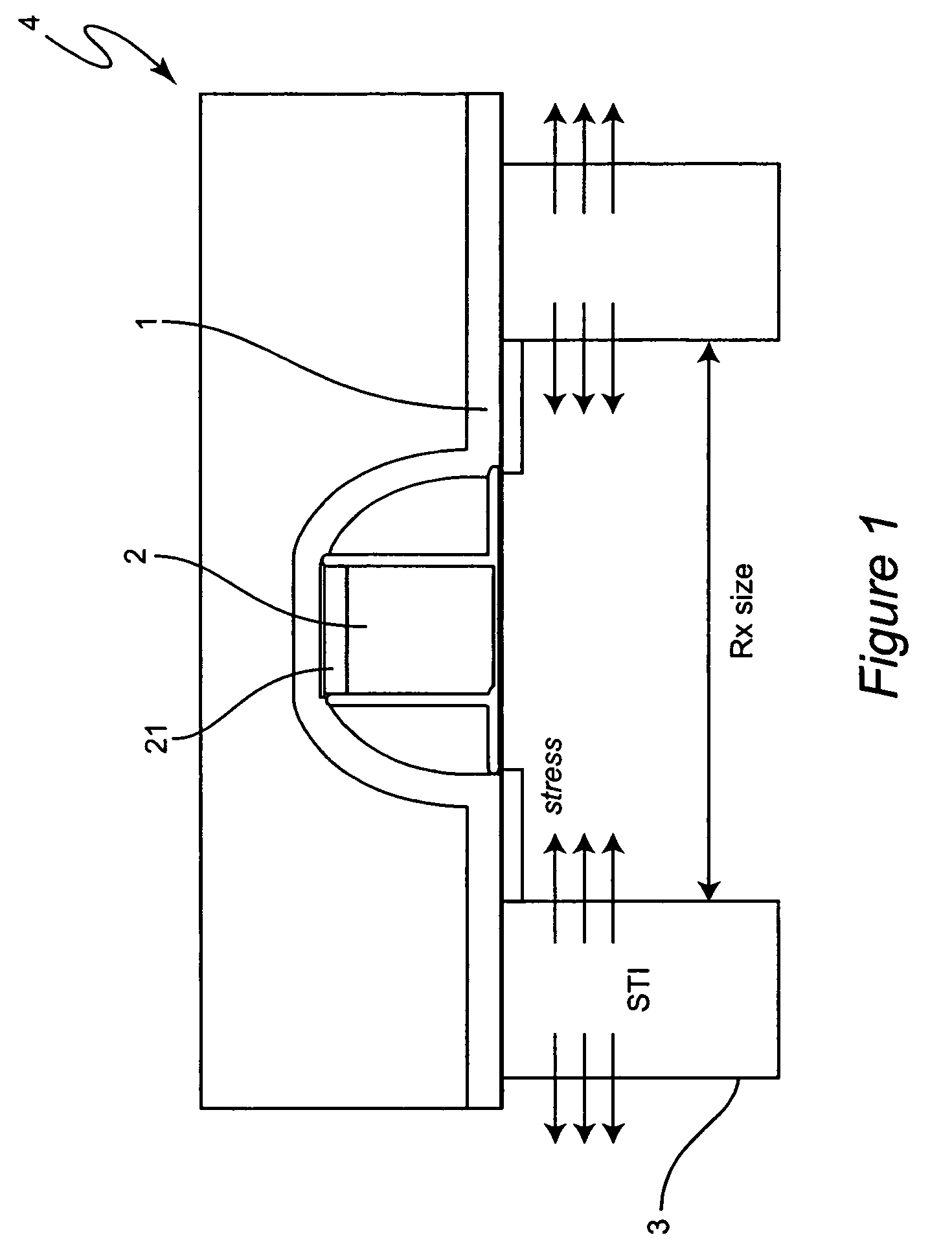
[0070]Device data was obtained that shows the drive current improvement compared to conventional films. FIGS. 3 and 4 show the electrical characteristics of the nFET and pFET. BTBAS nitride film can provide higher NFET drive current compared with devices with PECVD Tensile Nit film (and PECVD Compressive Nit film). There is also no degradation on the pFET drive current, for the film according to the inventive example. The nFET drive current improvement is dependent on the local strain, hence the device geometry and nitride thickness. In general, for a long width nFET device, BTBAS with 500 A in thickness can provide 8% nFET current improvement, with 750 A BTBAS giving extra 3% current improvement. There is also no degradation on the pFET drive current.
[0071]The FIG. 5 Iodlin da...
##ventive example 2
INVENTIVE EXAMPLE 2
[0072]In an RTCVD process, BTBAS and NH3 are reacted, under the following conditions:
[0073]
Carbon concentration:~6 to 10%Temperature650° C.Pressure140 torrDilane, disilane, hexachloro disilane?None
Films of thickness 500 or 750 angstroms are formed. Other film thicknesses may be formed.
PUM
| Property | Measurement | Unit |
|---|---|---|
| temperature | aaaaa | aaaaa |
| temperature | aaaaa | aaaaa |
| thickness | aaaaa | aaaaa |
Abstract
Description
Claims
Application Information
 - R&D
- Intellectual Property
- Life Sciences
- Materials
- Tech Scout
- Unparalleled Data Quality
- Higher Quality Content
- 60% Fewer Hallucinations
Browse by: Latest US Patents, China's latest patents, Technical Efficacy Thesaurus, Application Domain, Technology Topic, Popular Technical Reports.
© 2025 PatSnap. All rights reserved.Legal|Privacy policy|Modern Slavery Act Transparency Statement|Sitemap|About US| Contact US: help@patsnap.com


