Semiconductor light-emitting device
a technology of semiconductors and light-emitting devices, which is applied in the direction of semiconductor lasers, semiconductor/solid-state device details, instruments, etc., can solve the problems of particularly difficult ohmic contact, and achieve excellent ohmic contact
- Summary
- Abstract
- Description
- Claims
- Application Information
AI Technical Summary
Benefits of technology
Problems solved by technology
Method used
Image
Examples
first embodiment
[0047](First Embodiment)
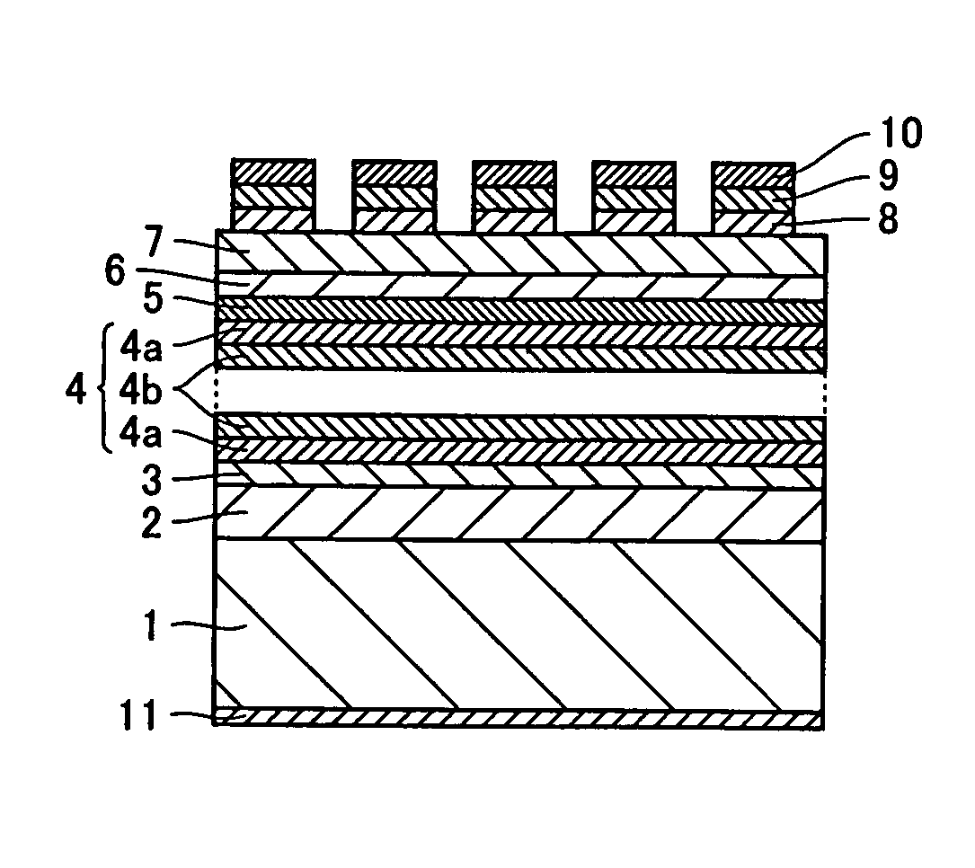
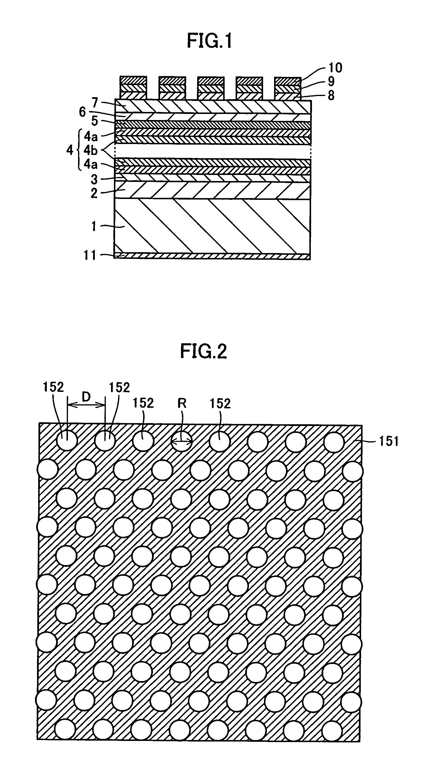
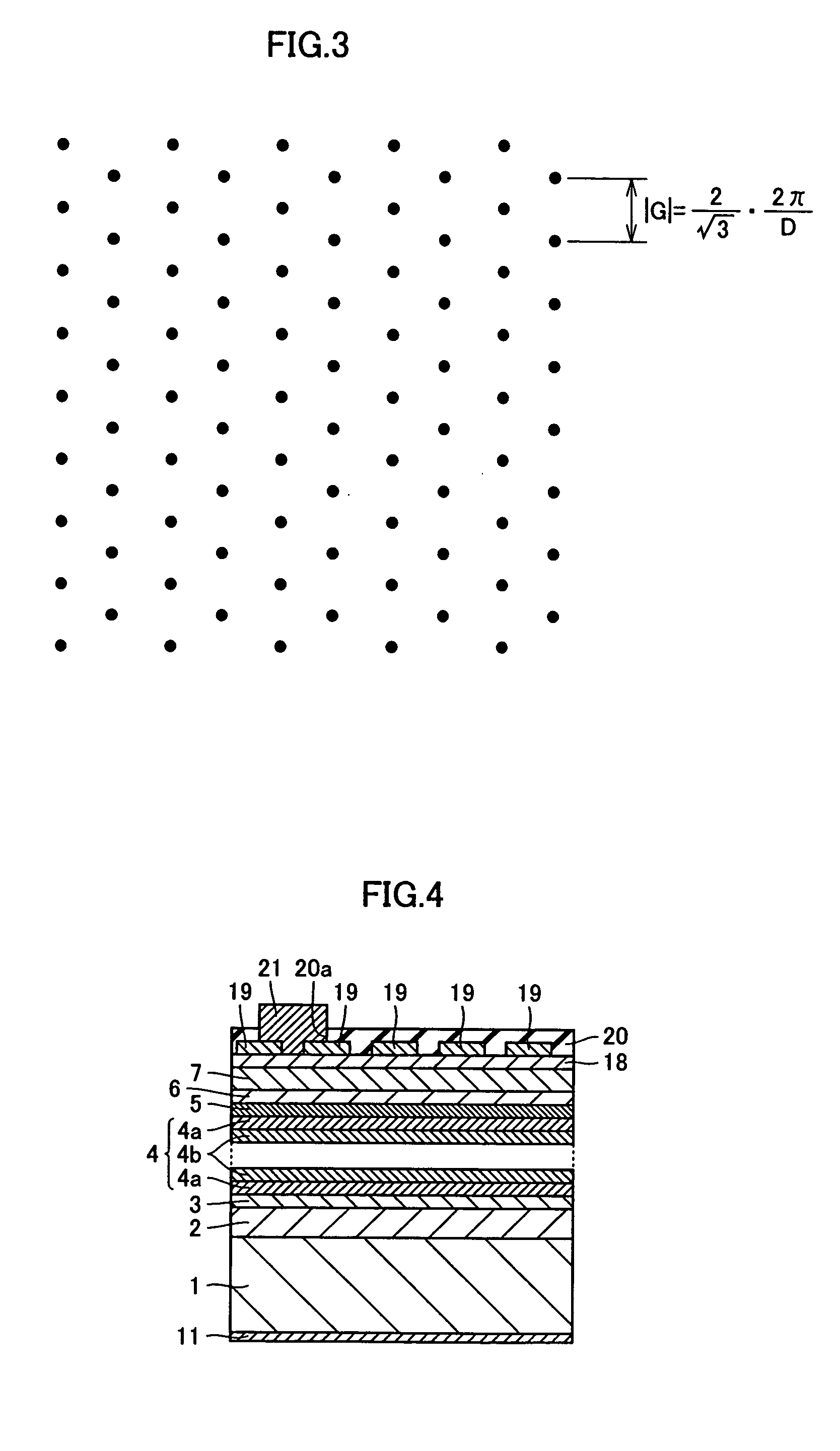
[0048]The structure of a nitride-based semiconductor LED according to a first embodiment of the present invention extracting light through a periodically formed electrode is described with reference to FIGS. 1 to 3.
[0049]In the nitride-based semiconductor LED according to the first embodiment, an n-type layer 2 of single-crystalline Si-doped GaN having a thickness of about 5 μm is formed on the (0001) Ga plane of an n-type GaN substrate 1 doped with oxygen or Si, as shown in FIG. 1. An n-type cladding layer 3 of single-crystalline Si-doped Al0.1Ga0.9N having a thickness of about 0.15 μm is formed on the n-type layer 2. A multiple quantum well (MQW) emission layer 4 having an MQW structure prepared by alternately forming six barrier layers 4a of single-crystalline undoped GaN each having a thickness of about 5 nm and five well layers 4b of single-crystalline undoped Ga0.9In0.1N each having a thickness of about 5 nm is formed on the n-type cladding layer 3. The...
second embodiment
[0066](Second Embodiment)
[0067]Referring to FIG. 4, a nitride-based semiconductor LED according to a second embodiment of the present invention is so formed that only an electrode 19 of a metal exhibiting a high plasma frequency has a periodic structure for extracting light through the electrode 19 having the periodic structure, dissimilarly to the aforementioned first embodiment.
[0068]According to the second embodiment, an ohmic electrode 18 of Pt having a thickness of about 1 nm is formed on the overall surface of a p-type contact layer 7, as shown in FIG. 4. The electrode 19, having a thickness of about 3 nm, of Al exhibiting a high plasma frequency is formed on the ohmic electrode 18 to have the periodic structure in the form of a triangular lattice similarly to that in the first embodiment shown in FIG. 2. The ohmic electrode 18 of Pt is superior to the electrode 19 of Al in ohmic property with respect to the p-type contact layer 7 of Mg-doped Ga0.95In0.05N. The electrode 19 co...
third embodiment
[0074](Third Embodiment)
[0075]Referring to FIG. 5, a nitride-based semiconductor LED according to a third embodiment of the present invention is provided with a p-type contact layer 37 having a periodic corrugated shape on its surface, for extracting light from the side formed with the corrugated shape.
[0076]In the nitride-based semiconductor LED according to the third embodiment, circular portions (cylindrical projection or recess portions) 152 in the form of a (two-dimensional) triangular lattice corresponding to those shown in FIG. 2 are periodically formed on the surface of the p-type contact layer 37 of Mg-doped Ga0.95In0.05N. In this case, the distance D between each pair of adjacent circular portions (cylindrical projection or recess portions) 152 is set to 660 nm, and the diameter R of each circular portion (cylindrical projection or recess portion) 152 is set to 330 nm. The nitride-based semiconductor LED is designed on the assumption that the wavelength of light emitted fr...
PUM
 Abstract
Description
Claims
Application Information
 - R&D
- Intellectual Property
- Life Sciences
- Materials
- Tech Scout
- Unparalleled Data Quality
- Higher Quality Content
- 60% Fewer Hallucinations
Browse by: Latest US Patents, China's latest patents, Technical Efficacy Thesaurus, Application Domain, Technology Topic, Popular Technical Reports.
© 2025 PatSnap. All rights reserved.Legal|Privacy policy|Modern Slavery Act Transparency Statement|Sitemap|About US| Contact US: help@patsnap.com


