In-situ cleaning of light source collector optics

a technology for light source collectors and optics, applied in the direction of cleaning using liquids, instruments, photomechanical equipment, etc., can solve the problems of loss of reflectivity and reduce the amount of light available for lithography

Inactive Publication Date: 2005-11-29
INTEL CORP
View PDF12 Cites 35 Cited by
  • Summary
  • Abstract
  • Description
  • Claims
  • Application Information

AI Technical Summary

Problems solved by technology

The eroded material may then coat the collector optics, resulting in a loss of reflectivity and reducing the amount of light available for lithography.

Method used


Image

  • In-situ cleaning of light source collector optics
  • In-situ cleaning of light source collector optics
  • In-situ cleaning of light source collector optics

Examples


Embodiment Construction

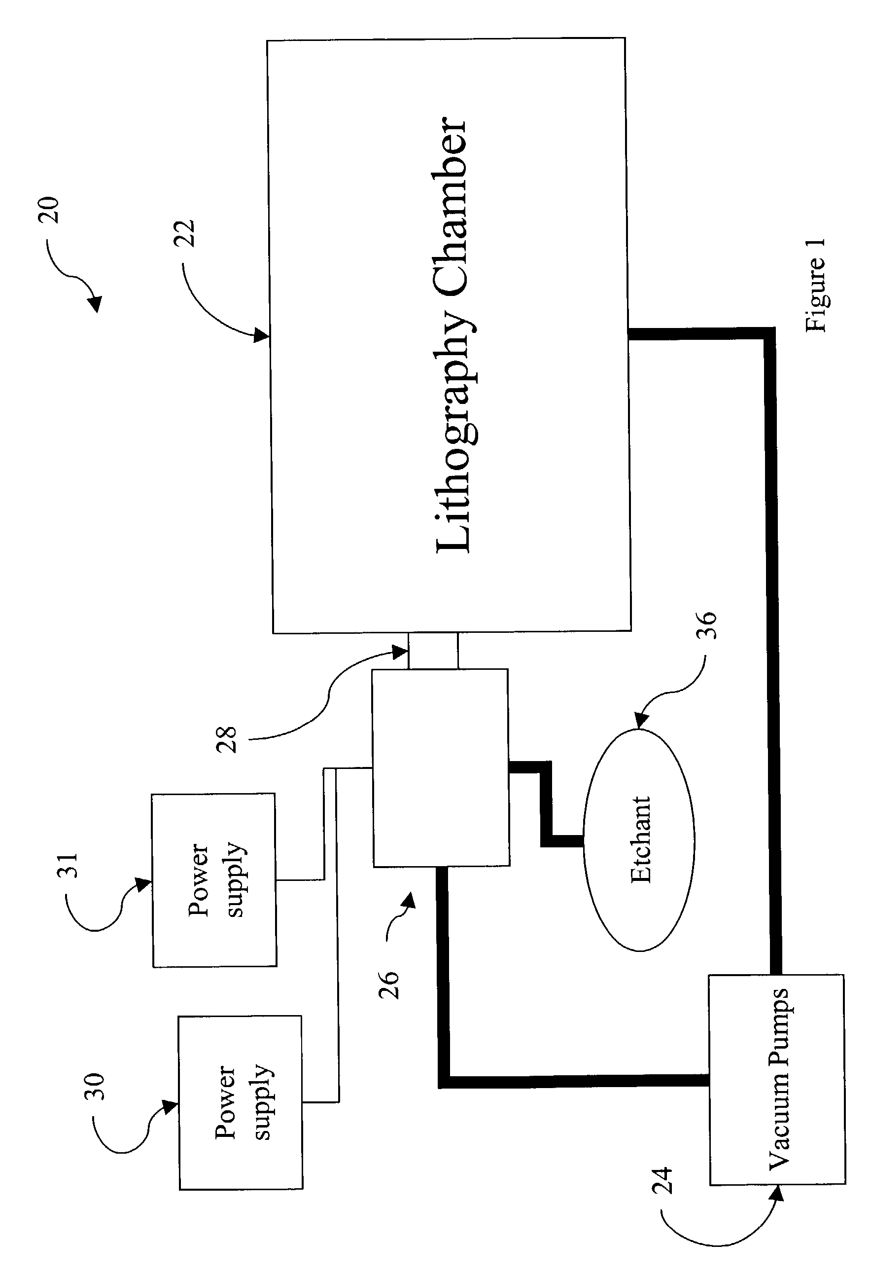
[0015]FIG. 1 shows a lithography system 20. The wafer with the light sensitive coating and the mask are placed in the lithography chamber 22. The pressure in the lithography chamber 22 is reduced to a near vacuum environment by vacuum pumps 24. A light source chamber 26, which houses a light source, is connected to the lithography chamber 22. The pressure in the light source chamber 26 is also reduced to a near vacuum environment by vacuum pumps 24. The light source chamber 26 and lithography chamber 22 are separated by a valve 28 that can be used to isolate the chambers 22, 26. This allows for different environments within each chamber.

[0016]The light source chamber 26 can be a EUV chamber, which houses a EUV light source. A power supply 30 is connected to the EUV chamber 26 to supply energy for creating a EUV photon emitting plasma, which provides EUV light for lithography. The light source chamber is evacuated by vacuum pumps 24.

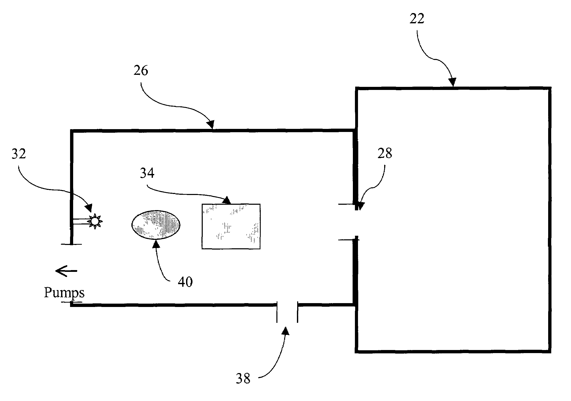
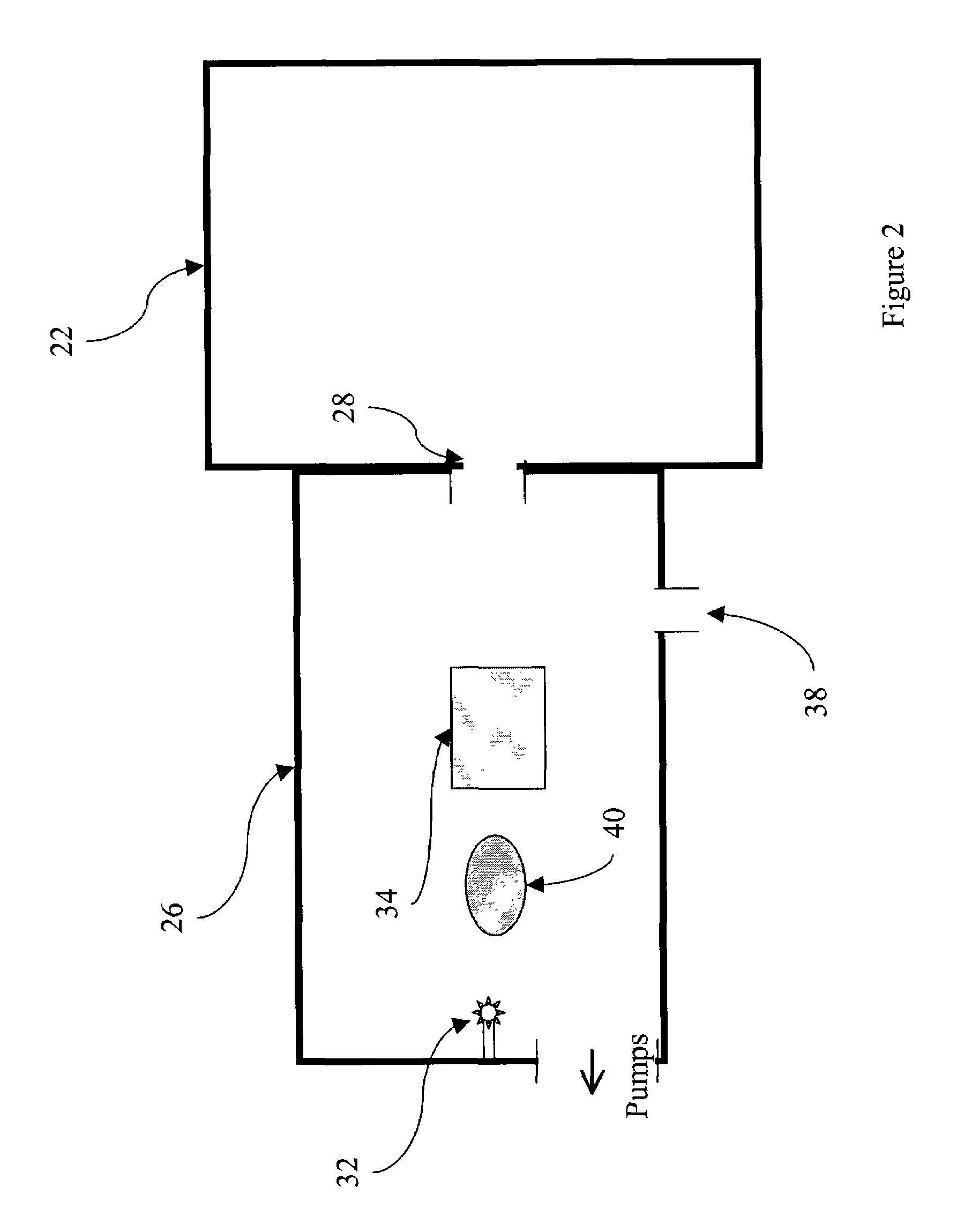
[0017]FIG. 2 shows the light source chamber 26 conn...


PUM

PropertyMeasurementUnit
wavelengthsaaaaaaaaaa

Abstract

A method and system for cleaning collector optics in a light source chamber. In producing, for example, extreme ultraviolet light for lithography, debris such as tungsten can accumulate on optical components near a light source in the light source chamber.
An etchant, such as a fluorine-containing gas, can be introduced into the light source chamber. The etchant is ionized via electrodes to generate free fluorine. The electrodes can be, for example, existing light source chamber components including the optical components. The fluorine can then react with the debris, forming gaseous compounds, which are pumped out of the light source chamber.

Description

[0001]This description relates to in-situ cleaning of light source collector optics.BACKGROUND[0002]Lithography is used in the fabrication of semiconductor devices. It is the technique by which the patterns that make up the circuitry of a chip are defined. In lithography, a light-sensitive material coats a wafer substrate, such as silicon, that is exposed to light at some wavelength to reproduce an image of the mask that is used to define each die on the wafer. The mask is usually referred to as a reticle in optical lithography, in that it is separated from the wafer by a series of objective lenses. When the wafer and mask are illuminated, the light-sensitive material, or photoresist, undergoes chemical reactions to produce a replicated pattern of the mask on the wafer. The patterns can then be manipulated in ways to transform the structure or properties of the wafer, which leads to the creation of various semiconductor devices and applications.[0003]The source of the light used in ...

Claims


Application Information

Patent Timeline
Patent Type & Authority Patents(United States)
IPC IPC(8): B08B7/00G03F7/20
CPCB08B7/0057G03F7/70925G21K1/06Y10S134/902
Inventor CHAN, MICHAELBRISTOL, ROBERTDOCZY, MARK
Owner INTEL CORP
Why Eureka
Try Eureka