Capacitor, capacitor equipped semiconductor device assembly, capacitor equipped circuit substrate assembly and electronic unit including semiconductor device, capacitor and circuit substrate

a technology of capacitors and semiconductor devices, which is applied in the direction of capacitor details, printed circuit non-printed electric components association, semiconductor/solid-state device details, etc., can solve the problems of increasing work time, increasing the space required for circuit substrates, and increasing the number of joining portions, so as to achieve stable electrical conduction and high thermal expansion coefficient

Inactive Publication Date: 2005-11-01
NGK SPARK PLUG CO LTD
View PDF14 Cites 46 Cited by
  • Summary
  • Abstract
  • Description
  • Claims
  • Application Information

AI Technical Summary

Benefits of technology

[0005]It is accordingly an object of the present invention to provide a capacitor, capacitor equipped semiconductor device assembly, capacitor equipped circuit substrate assembly and an electronic unit including a semiconductor device, capacitor and circuit substrate, which capacitor is free from the above-noted problem and can be assuredly installed between a semiconductor device such as a IC chip and a circuit substrate mainly made of insulating resin.
[0018]According to a further aspect of the present invention, there is provided an electronic unit comprising the above-described capacitor, a semiconductor device mounted on the front surface of the capacitor and having at a bottom surface a plurality of connecting terminals, and a circuit substrate having a first main surface on which the capacitor is mounted and a second main surface, wherein at least the first main surface and the second main surface are formed by insulating resin layers. By this, the capacitor and the semiconductor device mounted on the front surface of the capacitor are electrically connected to each other at a location between the first dielectric layer having a low thermal expansion coefficient and the bottom surface of the main body of the semiconductor device. The circuit substrate and the capacitor mounted on the first main surface of the circuit substrate are electrically connected to each other at a location between the insulating resin layer having a high thermal expansion coefficient and the second dielectric layer having a high dielectric constant. Due to this, the charge stored in the capacitor can be supplied to the circuit elements within the circuit device in the shortest distance and to the internal electrodes within the circuit substrate through relatively short conduction paths. Furthermore, the capacitor is not bent or curved even when subjected to thermal variations, and the electrical connecting portions among the three, i.e., the semiconductor device, capacitor and circuit substrate, are not broken, thus making it possible to attain stable electrical conduction.

Problems solved by technology

This causes a problem that the circuit substrate is required to have an increased space for disposition of the insulating resin layer.
A further problem of the circuit substrate is that there is a difficulty in disposition of an internal wiring and there is necessitated an increased work time for forming the recess and disposing the capacitor in the recess.
However, if a capacitor having connecting terminals at front and rear surfaces is disposed between an IC chip made of Si of a low thermal expansion coefficient and a circuit substrate made of insulating resin of a high thermal expansion coefficient to join the capacitor and the circuit substrate by way of the connecting terminals, there occurs a problem that a capacitor main body is bent or curved to cause some of joining portions to break due to the difference in the thermal expansion coefficient between the capacitor and circuit substrate and due to the fact that the capacitor is generally low in the Young's modulus.

Method used


Image

  • Capacitor, capacitor equipped semiconductor device assembly, capacitor equipped circuit substrate assembly and electronic unit including semiconductor device, capacitor and circuit substrate
  • Capacitor, capacitor equipped semiconductor device assembly, capacitor equipped circuit substrate assembly and electronic unit including semiconductor device, capacitor and circuit substrate
  • Capacitor, capacitor equipped semiconductor device assembly, capacitor equipped circuit substrate assembly and electronic unit including semiconductor device, capacitor and circuit substrate

Examples


Embodiment Construction

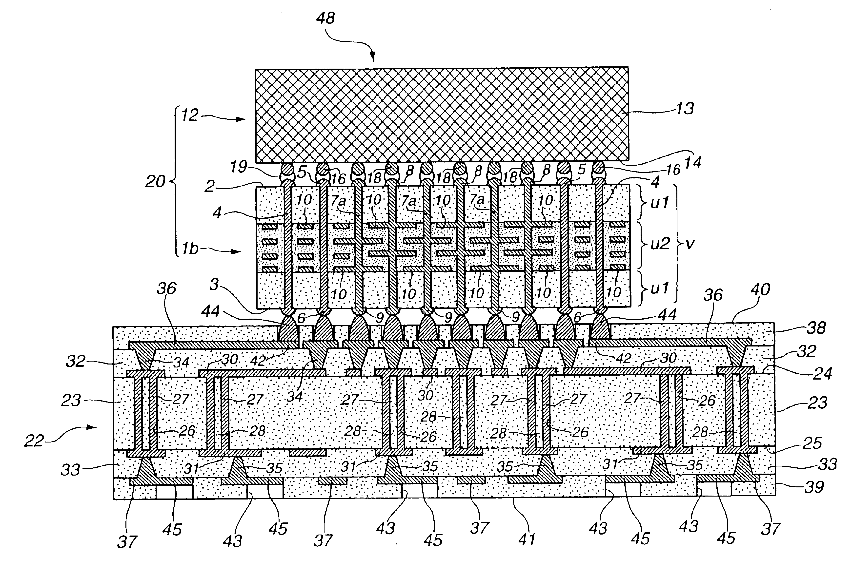
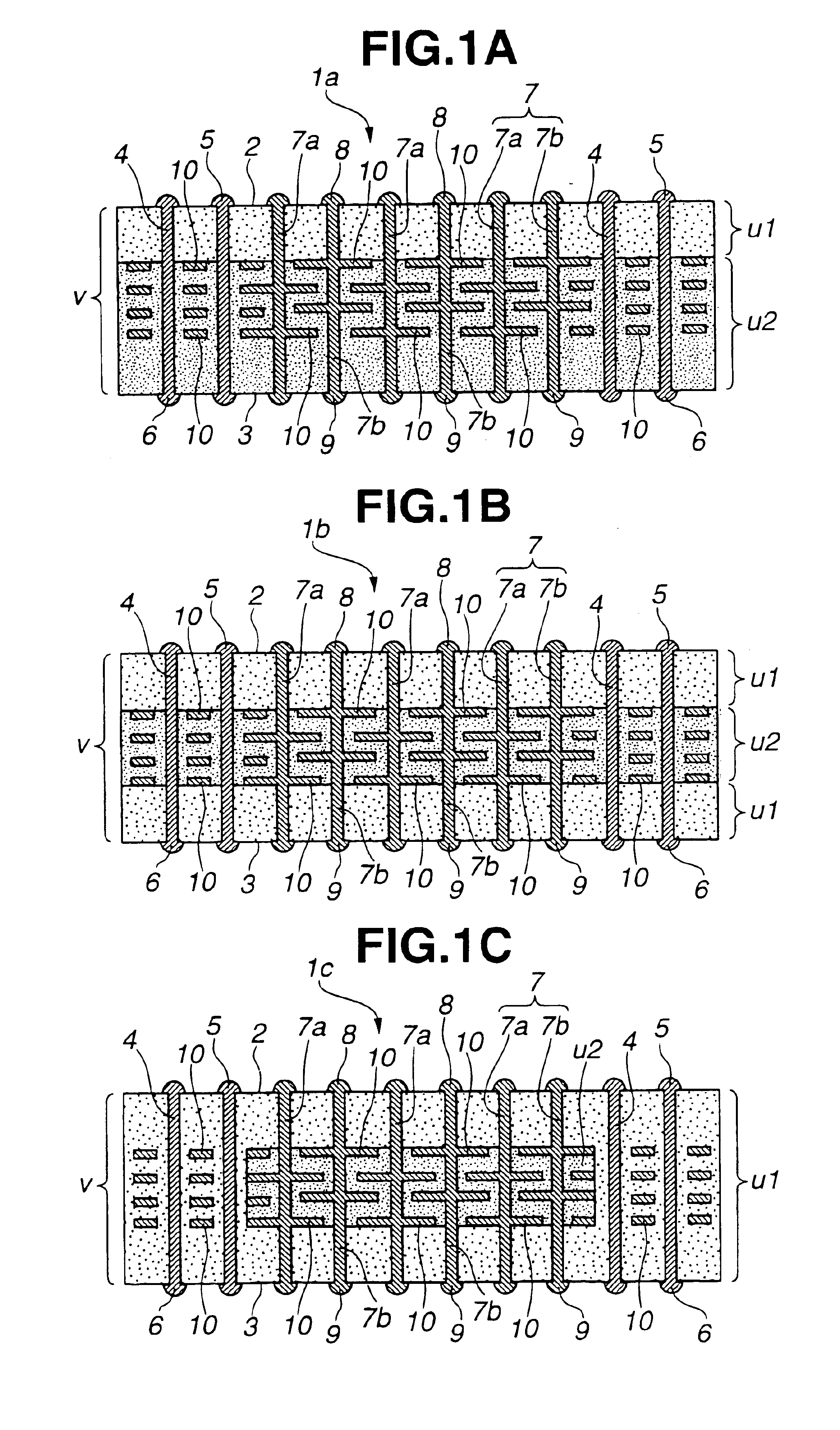
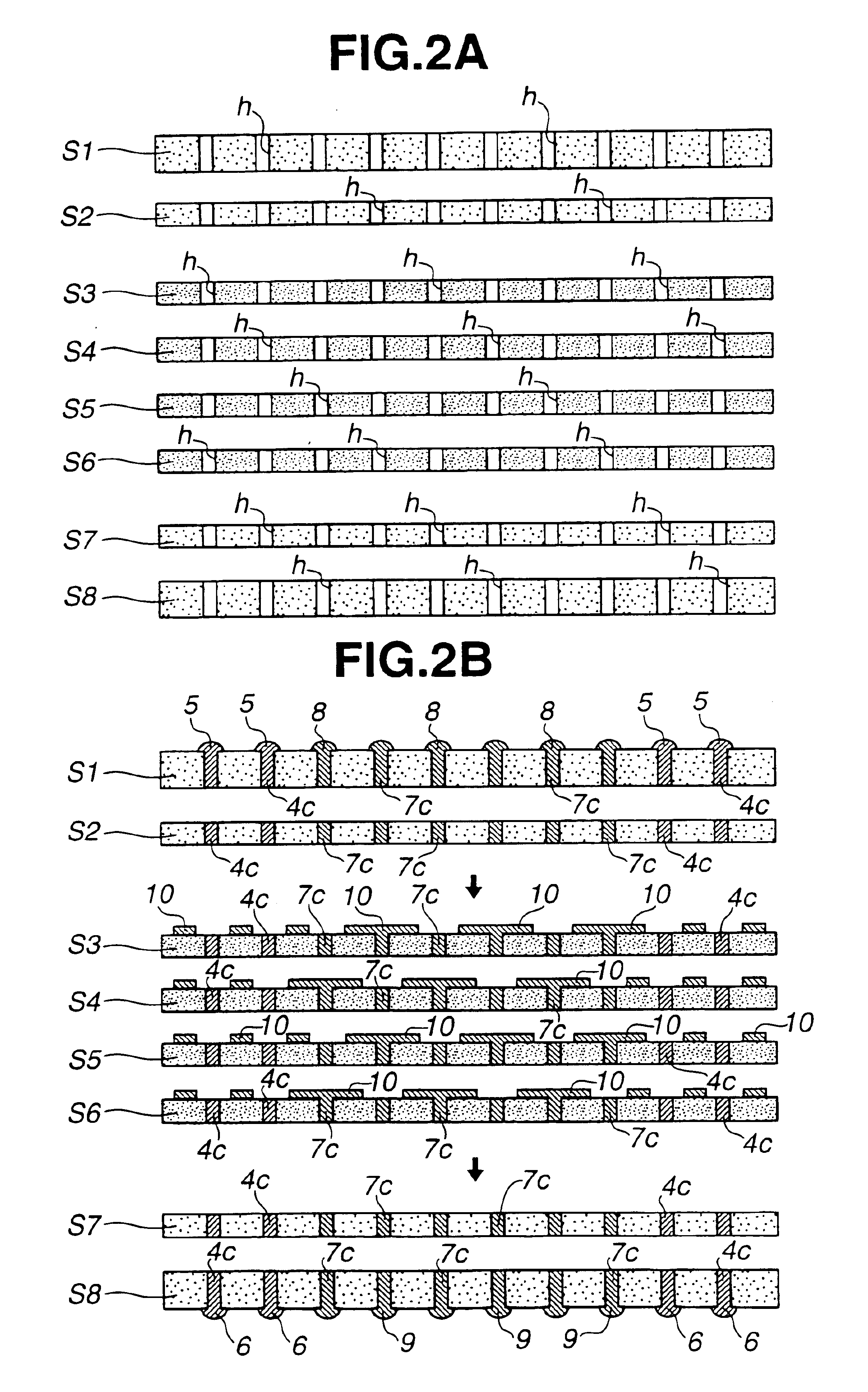
[0024]Referring first to FIG. 1A, a capacitor 1a according to an embodiment of the present invention includes a capacitor main body v having a front surface 2 on which a semiconductor device which will be described later is to be mounted and a rear surface 3 at which the capacitor 1a is to be mounted on a first main surface of a circuit substrate which will be described later, a plurality of front surface side bumps 5, 8 formed on the front surface 2 and a plurality of rear surface side bumps 6, 9 formed on the rear surface 3.

[0025]The capacitor main body v has a square or rectangular shape when observed in a plan view and includes a first dielectric layer u1 positioned on a front surface 2 side and having a low thermal expansion coefficient and a high Young's modulus (200 GPa or larger) and a second dielectric layer u2 positioned on a rear surface 3 side and having a higher thermal expansion coefficient and a higher dielectric constant than the first dielectric layer u1.

[0026]The f...


PUM


Abstract

A capacitor includes a capacitor main body having a front surface on which a semiconductor device is to be mounted and a rear surface at which the capacitor main body is to be mounted on a first main surface of a circuit substrate, a plurality of internal electrodes disposed within the capacitor main body, and a plurality of via conductors penetrating the capacitor main body between the front surface and the rear surface and electrically connected to the internal electrodes, wherein the capacitor main body has a first dielectric layer located on a side of the capacitor main body closer to the front surface and a second dielectric layer located on a side of the first dielectric layer closer to the rear surface, the second dielectric layer having a higher thermal expansion coefficient and a higher dielectric constant than the first dielectric layer.

Description

BACKGROUND OF THE INVENTION[0001]The present invention relates to a capacitor, capacitor equipped semiconductor device assembly, capacitor equipped circuit substrate assembly and an electronic unit including a semiconductor device, capacitor and circuit substrate.[0002]Recently, it has been proposed a circuit substrate equipped with an IC chip mounted capacitor, the IC chip being not directly connected to the circuit substrate but connected to the same by interposing therebetween the capacitor that is mounted in a recess of the circuit substrate for the purpose of providing the IC chip with a good electric power supply while removing noise as disclosed in Unexamined Japanese Patent Publication No. 2000-349225.SUMMARY OF THE INVENTION[0003]However, in case of the above-described circuit substrate equipped with the IC chip mounted capacitor, the capacitor needs be mounted in the recess of the circuit substrate while being surrounded by an insulating resin layer. This causes a problem ...

Claims


Application Information

Patent Timeline
IPC IPC(8): H01G4/30H05K1/16H05K1/14H01G2/06H01L23/498H01L23/50H01L25/00H05K1/18
CPCH01G2/065H01L23/49822H01L23/49833H01L23/50H05K1/162H01G4/30H01L2224/16235H01L2224/16H01L2924/01046H01L2924/01078H01L2924/01079H01L2924/09701H01L2924/15174H01L2924/15311H01L2924/19103H05K1/141H05K3/4688H05K2201/068H05K2201/10378H01L2224/05573H01L2224/13025H01L2224/05611H01L2924/00014H01L2224/05644H01L2224/05647H01L2224/05655H01L2224/05664H01L2224/05666H01L2224/05684
Inventor OTSUKA, JUNSATO, MANABUKIMURA, YUKIHIRO
Owner NGK SPARK PLUG CO LTD
Why Eureka
Try Eureka