Magnetic cell and magnetic memory
a magnetic memory and cell technology, applied in the field of magnetic memory and cell, can solve the problems of insufficient generation of magnetic field, difficult localization,
- Summary
- Abstract
- Description
- Claims
- Application Information
AI Technical Summary
Benefits of technology
Problems solved by technology
Method used
Image

Examples
examples
[0217]Hereafter, the embodiment of the invention will be explained in more detail, referring to examples.
first example
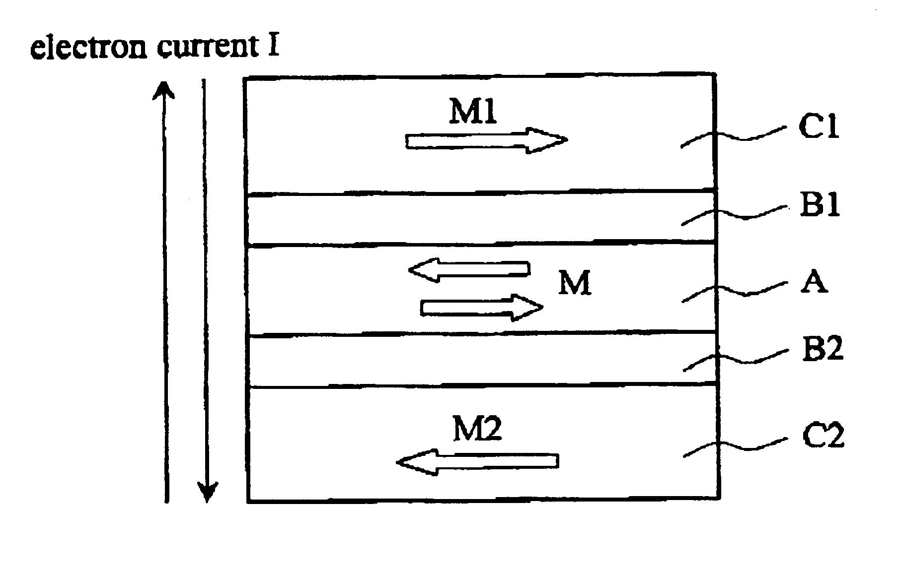
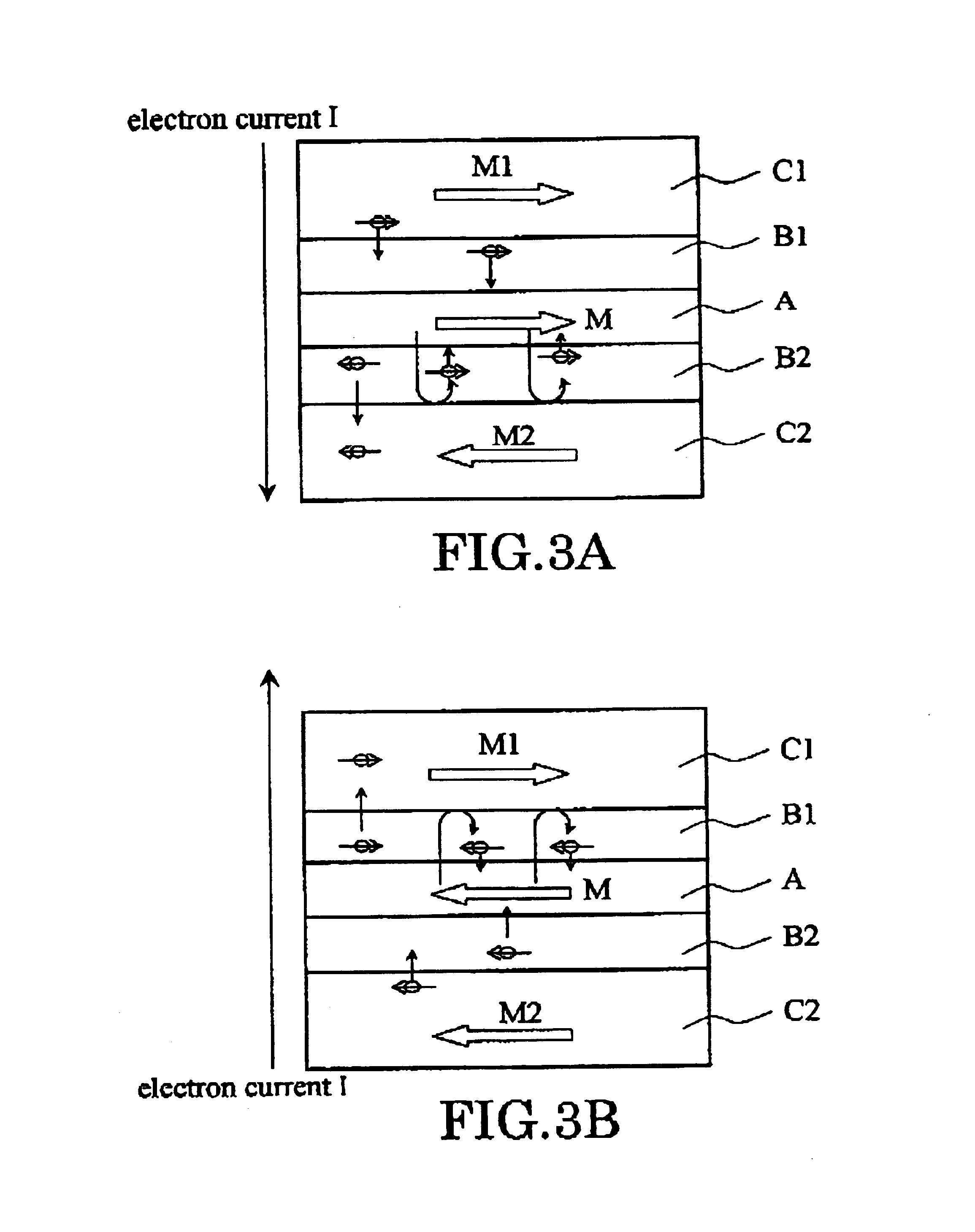
[0218]FIG. 29A is a schematic diagram showing the principal cross-sectional structure of the magnetic cell of this example, and FIG. 29B is a schematic diagram showing the principal cross-sectional structure of the magnetic cell of the comparative example.
[0219]That is, the magnetic cell of this example (sample I) has the structure where the electrode EL 1, the magnetically fixed layer C1, the intermediate layer B1, the magnetic recording layer A, intermediate-layer B2, the magnetically fixed layer C2, and the electrode EL 2 are laminated. Moreover, the magnetic cell of the comparative example (sample II) has the structure where the electrode EL 1, the magnetic recording layer A, the intermediate layer B, the magnetically fixed layer C, and the electrode EL2 are laminated. The material and the thickness of each layer are as the following:
[0220]Sample I: EL1(Cu) / C1(Co:20 nm) / B1(Cu:10 nm) / A(Co: 3 nm) / B2(Cu:6 nm) / C2(Co:20 nm) / EL2 (Cu)
[0221]Sample II:EL1(Cu) / A(Co:3 nm) / B(Cu:6nm) / C (Co: ...
second example
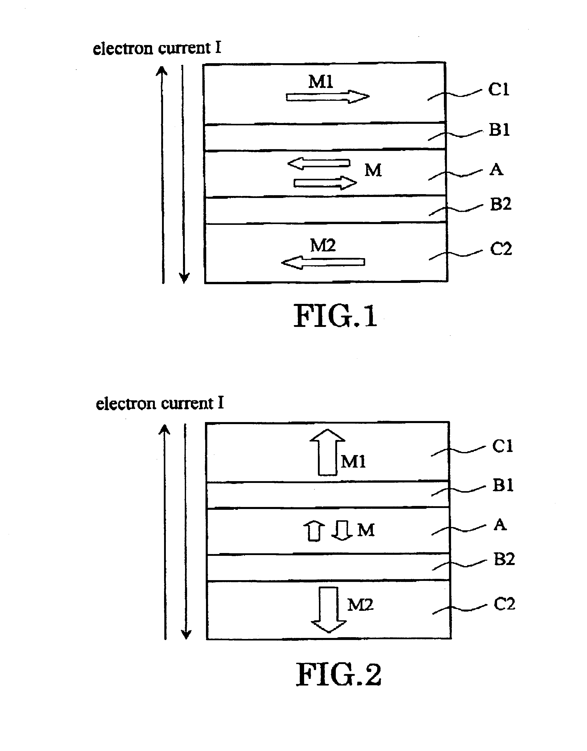
[0225]Next, the example of the magnetic cell of the structure expressed in FIG. 15 will be explained as the second example of the invention. In addition, in this example, the magnetic cell of the laminated structure which was reversed the upper and lower sides to FIG. 15 was made as an experiment.
[0226]First, the lower electrode EL 1 which consists of tantalum (Ta) and copper (Cu) was formed on the wafer by using the ultrahigh-vacuum sputtering equipment. PtMn 20 nm (the antiferromagnetic layer AF1), CoFe 5 nm (the magnetic layer FM), Ru 1 nm (the non-magnetic layer AC), CoFe 2 nm (the magnetically fixed layer C1), Cu 3 nm (the intermediate layer B1), CoFe 2 nm (the magnetic recording layer A), Cu 3 nm (the intermediate-layer B-2), CoFe 4 nm (the magnetically fixed layer C2), and PtMn 20 nm (the antiferromagnetic layer AF2) were formed on the bottom electrode EL 1. Furthermore, the laminated film which consists of copper (Cu) and tantalum (Ta) was formed on the cell.
[0227]Unidirecti...
PUM
 Abstract
Description
Claims
Application Information
 - R&D
- Intellectual Property
- Life Sciences
- Materials
- Tech Scout
- Unparalleled Data Quality
- Higher Quality Content
- 60% Fewer Hallucinations
Browse by: Latest US Patents, China's latest patents, Technical Efficacy Thesaurus, Application Domain, Technology Topic, Popular Technical Reports.
© 2025 PatSnap. All rights reserved.Legal|Privacy policy|Modern Slavery Act Transparency Statement|Sitemap|About US| Contact US: help@patsnap.com