
Semiconductor device for low voltage protection with low capacitance

Inactive Publication Date: 2005-10-18
TECCOR ELECTRONICS
View PDF51 Cites 37 Cited by
  • Summary
  • Abstract
  • Description
  • Claims
  • Application Information

AI Technical Summary

Benefits of technology

[0019]In accordance with another feature of the invention, a deep base is provided to thereby make the mid-region of the substrate thinner. The mid-region of the substrate functions in the four-layer device as a base of one of the regenerative-connected transistors of the thyristor device. With a thinner transistor base, the gain of the device is higher, thereby increasing the operational speed of the thyristor.
[0021]In yet another embodiment, a low voltage thyristor device is formed as a center-fired device in which the buried region is formed offset from the emitter, but generally centered in the chip. This arrangement not only allows an increased device current to flow, but also facilitates assembly of the packaged device. By placing the buried region in the center of the semiconductor chip and utilizing two symmetrically oriented metal contacts, the chip self centers itself to a lead frame when reflow soldered thereto.
[0023]According to another embodiment, high impurity concentration buried regions are used to not only achieve a low breakdown voltage, but the buried regions are constructed utilizing cross-sectionally small areas to reduce device capacitance. The device can thus be used for protecting lines carrying high speed digital signals. An additional feature of this embodiment is that the buried regions are formed at various locations with respect to the emitter region, such that full conduction over the entire emitter area is achieved faster, thereby reducing the voltage overshoot of the device. In accordance with a described embodiment, the emitter of the device is fabricated with a peripheral edge or perimeter having indentions or cutouts formed therein. Formed below such cutouts are corresponding buried regions. The location of the buried regions with respect to the emitter allow carriers emitted from the buried regions to flow to essentially the entire, if not all, of the emitter area, thereby providing full turn on of the emitter. This allows high current densities to be accommodated during turn on of the device without causing “bottle-neck” locations of the current.

Problems solved by technology

While low-voltage digital lines, such as those driven by 5-volt TTL drivers are extensively employed in computerized and other equipment, such lines have not yet found a large application in outside installations.
In any event, even after fine tuning the processes so as to prevent short circuiting between the buried region and the emitter, the yield of workable devices is low, and thus such devices become costly.
Another problem attendant with upward migration of the junction of the buried region is that the base region under the emitter becomes thinner.
A thinner base region adversely affects the ability to control a desired holding current.
While numerous five-pin primary protection modules are commercially available to provide primary protection, there is a limited selection of five-pin secondary protection modules providing secondary protection.
This imposes additional constraints not currently satisfied by currently available devices and circuits.

Method used


Image

  • Semiconductor device for low voltage protection with low capacitance
  • Semiconductor device for low voltage protection with low capacitance
  • Semiconductor device for low voltage protection with low capacitance

Examples


Embodiment Construction

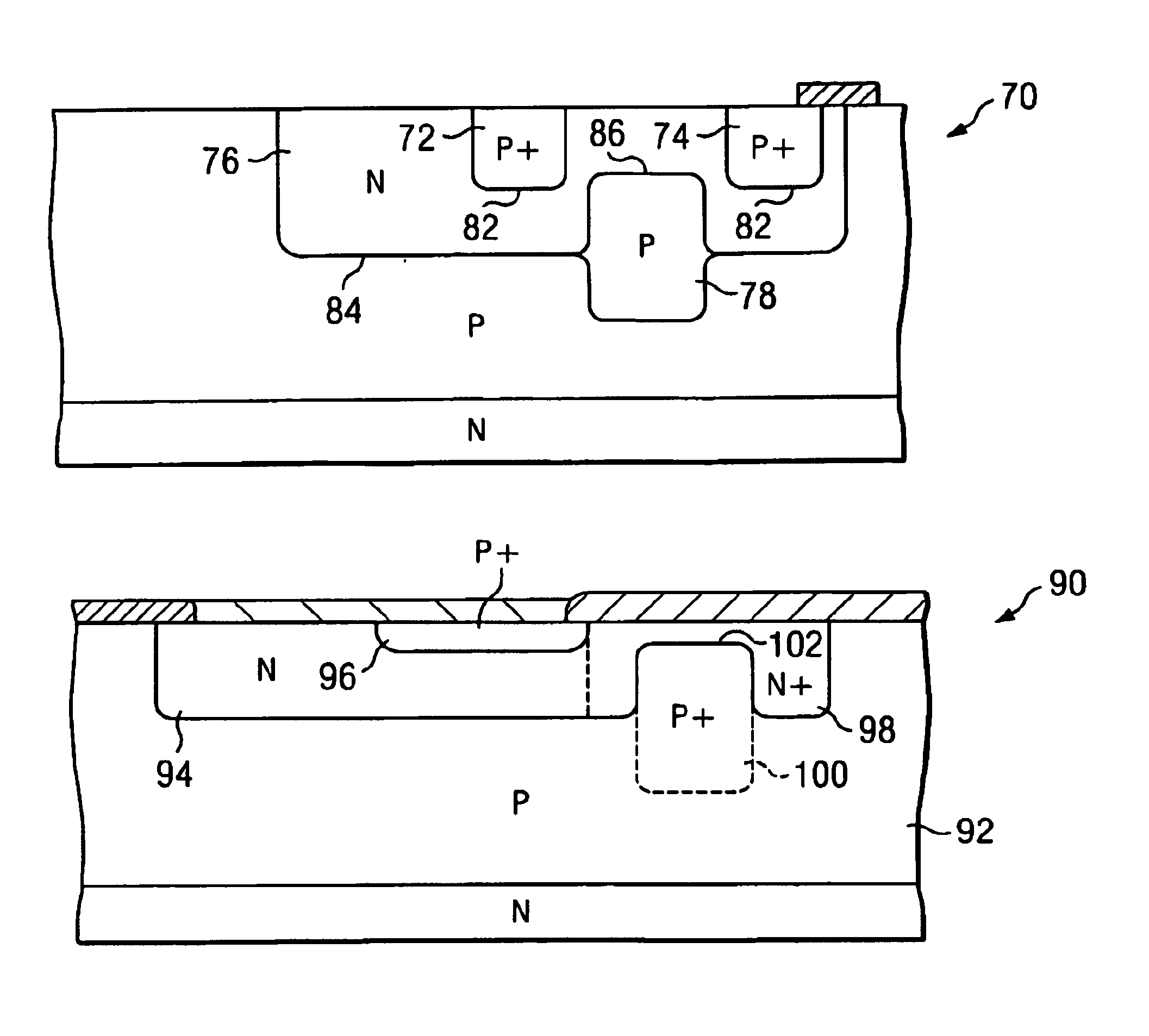
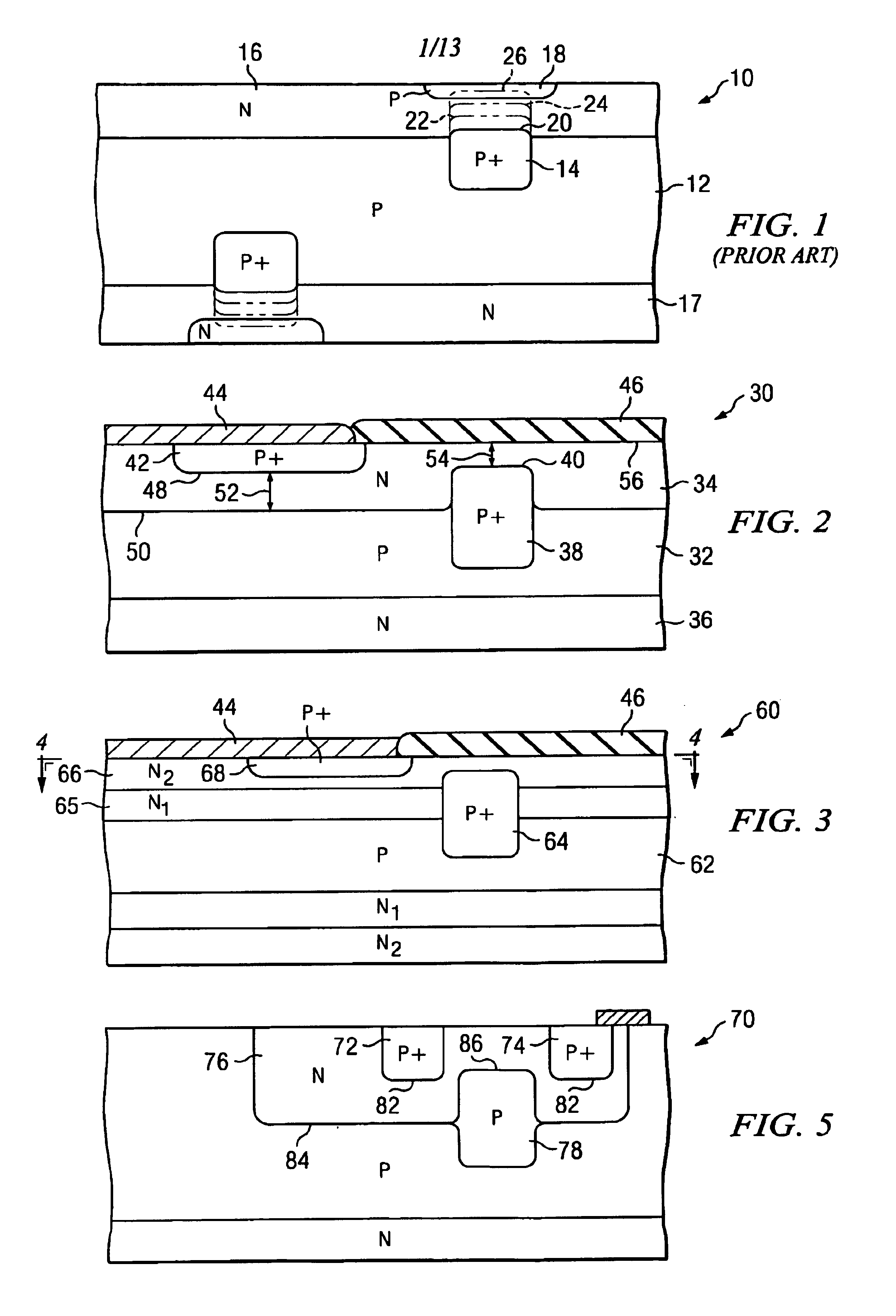
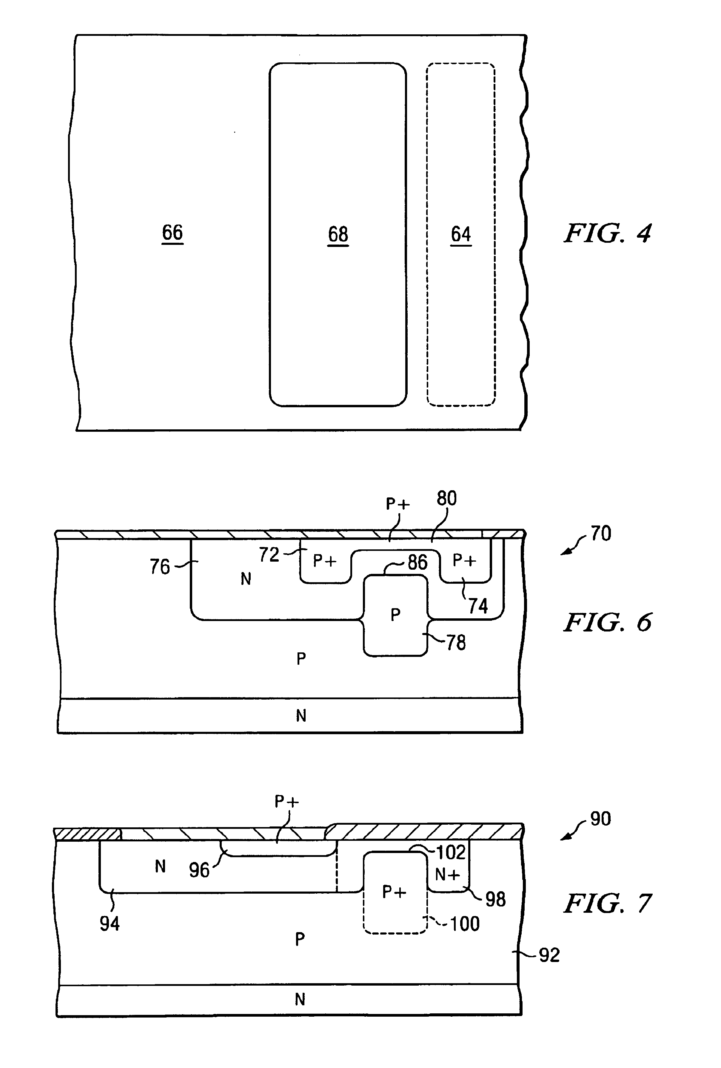
[0054]FIG. 2 illustrates the principles and concepts of one embodiment of the invention. A single four-layer unidirectional device 30 is illustrated. Two such devices (a top surface and bottom surface device) can be formed in the semiconductor substrate to provide bidirectional current flow capabilities. The device 30 is formed in the top surface of a starting silicon substrate 32 of the P-type. Region 32 defines both the mid-region of the four-layer thyristor, and a base of a NPN transistor. An N-type base region 34 for one device is formed in the top surface of the wafer, and a second N-type base region 36 for a second device (not shown) is formed in the bottom surface of the wafer. A heavily doped buried region 38 is formed in the substrate 32, preferably by standard semiconductor diffusion techniques and before either base region 34 or 36 is formed. The buried region 38 is formed by diffusing boron atoms for about three days, resulting in a surface concentration of about 1019 at...


PUM


Abstract

A semiconductor thyristor device that incorporates buried region breakdown junctions laterally offset from an emitter region. By spacing the buried regions around the emitter region, current carriers emitted from the buried regions are distributed over a large area of the emitter region, thereby providing a high current capability during initial turn on of the device. In order to achieve low breakover voltage devices, the buried regions are characterized with high impurity concentrations, with the breakdown junctions located near the surface of the chip. The low voltage thyristor device minimizes the area of high dopant concentration junctions, thus minimizing the chip capacitance and permitting high speed, low voltage signal operation.

Description

RELATED APPLICATIONS[0001]This patent application is a continuation-in-part of U.S. national stage application Ser. No. 09 / 958,987 filed Oct. 12, 2001, now abandoned, which claims priority to PCT international application PCT / US01 / 04906, filed Feb. 15, 2001, which international application is a continuation-in-part of pending U.S. application Ser. No. 09 / 504,224, filed Feb. 15, 2000, now U.S. Pat. No. 6,531,717, entitled “Very Low Voltage Actuated Thyristor With Centrally-Located Offset Buried Region”, which is a continuation-in-part patent application of U.S. application Ser. No. 09 / 260,328, filed Mar. 1, 1999 now U.S. Pat. No. 6,084,253, issued Jul. 4, 2000, the entire subject matter of the applications and patent of which is incorporated herein by reference.TECHNICAL FIELD OF THE INVENTION[0002]The present invention relates in general to thyristors and other four-layer devices, and more particularly to the fabrication of thyristor devices having low breakover voltages.BACKGROUND ...

Claims


Application Information

Patent Timeline
IPC IPC(8): H01L29/66H01L29/747H01L29/87
CPCH01L29/747H01L29/87
Inventor CASEY, KELLY C.TURNER, JR., ELMER L.
Owner TECCOR ELECTRONICS
Learn More