
Method of forming semiconductor device with non-conformal liner layer that is thinner on sidewall surfaces

a technology of sidewall surface and semiconductor device, which is applied in the direction of semiconductor devices, basic electric elements, electrical equipment, etc., can solve the problems of junction leakage, structural damage, and the surface of a chip alone cannot have enough space to accommodate all interconnections, and achieve the effect of reducing junction leakag

Inactive Publication Date: 2005-09-13
PROMOS TECH INC
View PDF8 Cites 11 Cited by
  • Summary
  • Abstract
  • Description
  • Claims
  • Application Information

AI Technical Summary

Benefits of technology

[0015]Accordingly, one object of the present invention is to provide a method of forming a contact opening capable of reducing junction leakage resulting from a damaged substrate surface in a conventional bitline contact opening fabrication process.
[0016]A second object of this invention is to provide a method of forming a contact opening capable of reducing the complexity in fabricating a conventional bitline contact opening.
[0019]This invention utilizes a tilted or a vertical ion implantation to reduce the thickness of the liner layer that is subsequently formed on the sidewall of a gate structure when compared with the liner layer on the substrate surface. Ultimately, a wider gap is produced between the neighboring gate structures and hence the process window for a subsequent etching or deposition is increased.
[0020]Furthermore, there is no need to etch the liner layer in this invention. Hence, uniformity of the liner layer on the substrate can be ensured and damages to the substrate surface due to over-etching can be avoided.
[0021]In addition, the method for fabricating a contact opening according to this invention is capable of preventing any damage to the substrate surface (the doped region), junction leakage is greatly minimized. Moreover, with damage to the substrate surface reduced, ion implantation for restoring dopant concentration is no longer necessary. In other words, the contact opening fabrication process is very much simplified.

Problems solved by technology

As the level of integration of integrated circuits increases, the surface of a chip alone can hardly have sufficient area for accommodating all the interconnects.
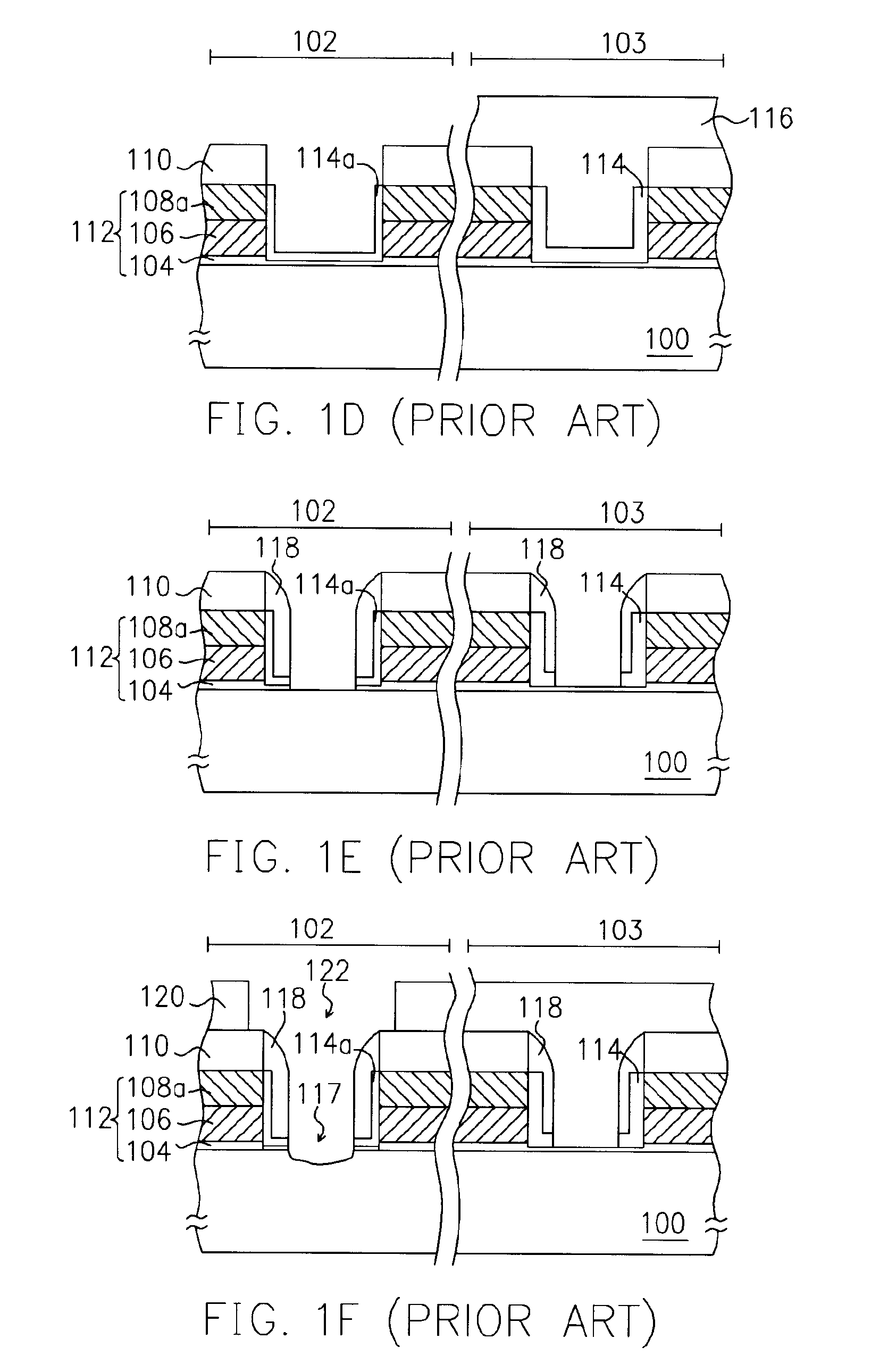
However, this practice may cause over-etching of the substrate 100 leading to some structural damage as shown by the numeral 117 in FIG.
Hence, damaging the region 117 may lead to junction leakage problems.
Therefore, the processing step is not only more complicated but may also intensify short channel effect.

Method used


Image

  • Method of forming semiconductor device with non-conformal liner layer that is thinner on sidewall surfaces
  • Method of forming semiconductor device with non-conformal liner layer that is thinner on sidewall surfaces
  • Method of forming semiconductor device with non-conformal liner layer that is thinner on sidewall surfaces

Examples


Embodiment Construction

[0026]Reference will now be made in detail to the present preferred embodiments of the invention, examples of which are illustrated in the accompanying drawings. Wherever possible, the same reference numbers are used in the drawings and the description to refer to the same or like parts.

[0027]FIGS. 2A through 2G are schematic cross-sectional views showing the progression of steps for producing a contact opening according to one preferred embodiment of this invention. As shown in FIG. 2A, a substrate 100 with a plurality of conductive structures 112 each having a cap layer 110 thereon is provided. In FIG. 2A, the region labeled 102 is the location for forming a bitline contact and the region labeled 103 is the location having no bitline contact. In other words, the region 102 is a prescribed area within a memory cell region for forming a bitline contact. On the other hand, the region 103 is a prescribed area within a peripheral circuit region or an area within the memory cell region ...


PUM


Abstract

A method of forming a contact opening is provided. First, a substrate having a plurality of conductive structures formed thereon is provided. An ion implantation is performed. Thereafter, a thermal treatment is carried out to form a liner layer on the sidewall of the conductive structure and the exposed substrate. The liner layer on the sidewall of the conductive structure has a thickness smaller than the liner layer on the substrate surface. A spacer is formed on each side of the conductive structure and then an insulation layer is formed over the substrate. The insulation layer is patterned to form a contact opening between two neighboring conductive structures. Since the liner layer on the sidewall of the conductive structures is already quite thin, there is no need to reduce thickness through an etching operation and uniformity of the liner layer on the substrate can be ensured.

Description

CROSS REFERENCE TO RELATED APPLICATIONS[0001]This application claims the priority benefit of Taiwan application serial no. 92116356, filed Jun. 17, 2003.BACKGROUND OF INVENTION[0002]1. Field of the Invention[0003]The present invention generally relates to a process of manufacturing semiconductor devices. More particularly, the present invention relates to a method of forming contact openings and a method of forming semiconductor devices.[0004]2. Description of the Related Art[0005]With rapid advancement in semiconductor fabrication technologies, the size of semiconductor devices has shrunk to deep sub-micron levels. As the level of integration of integrated circuits increases, the surface of a chip alone can hardly have sufficient area for accommodating all the interconnects. To provide necessary interconnects after device miniaturization, a design having two or more metallic interconnects is routinely used in very large scale integration (VLSI) packages. However, to connect two met...

Claims


Application Information

Patent Timeline
IPC IPC(8): H01L21/02H01L21/469H01L21/4763H01L21/477H01L21/3205H01L21/31H01L21/336H01L21/60H01L21/768
CPCH01L21/76838H01L21/76897H01L29/6656
Inventor YEH, FANG-YUCHEN, CHUN-CHE
Owner PROMOS TECH INC
Learn More