
Gated diode with non-planar source region

a gated diode and source region technology, applied in the direction of diodes, semiconductor devices, electrical apparatus, etc., can solve the problems of undesirable junction leakage, reduced driving current, and not always working perfectly of the mosfet gated diode, so as to reduce the maximum electric field, reduce the encroachment or lateral scattering of dopants, and reduce junction leakage

Active Publication Date: 2008-10-02
TAIWAN SEMICON MFG CO LTD
View PDF7 Cites 5 Cited by
  • Summary
  • Abstract
  • Description
  • Claims
  • Application Information

AI Technical Summary

Benefits of technology

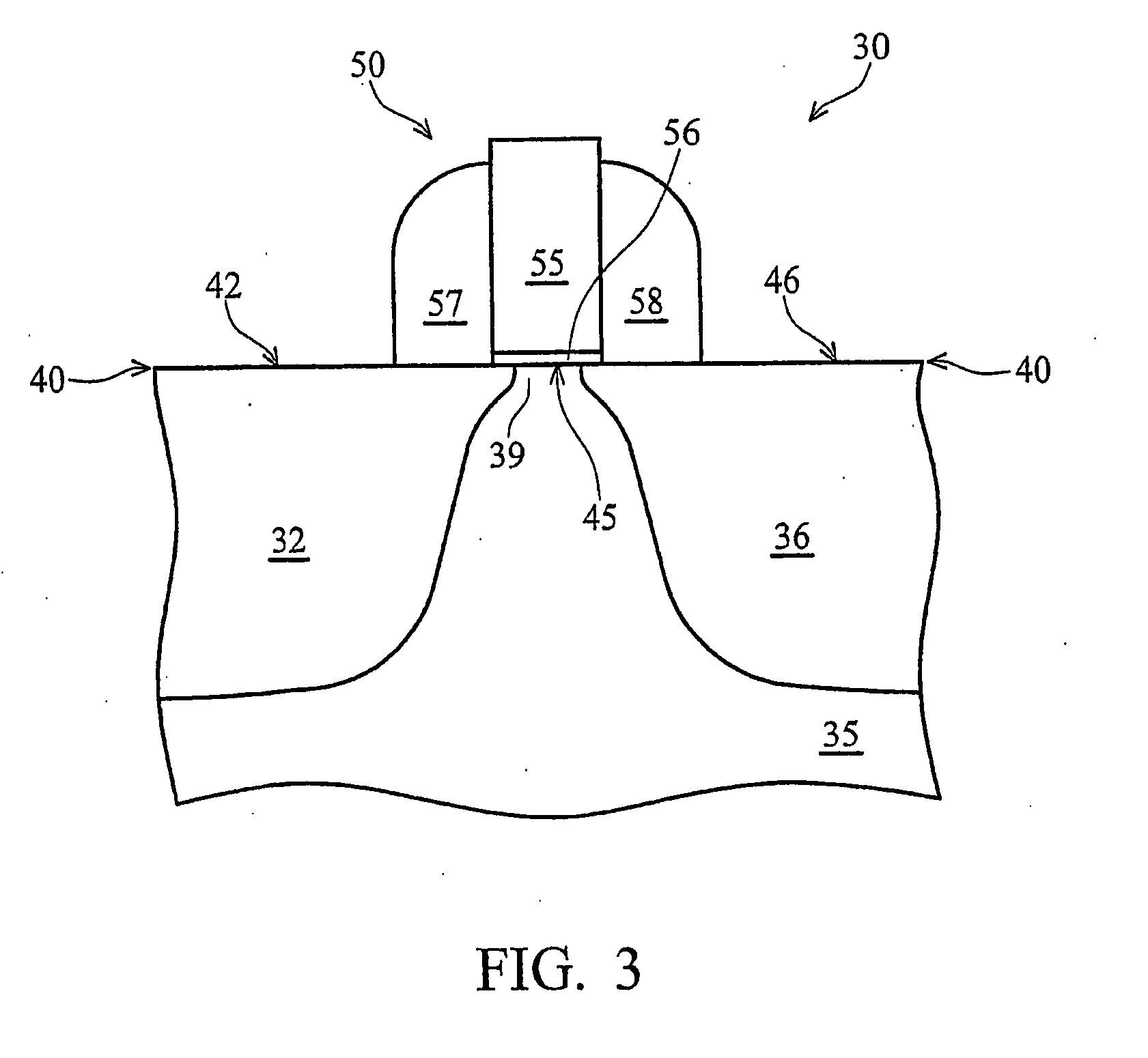
[0013]An advantage of a preferred embodiment of the present invention is that it reduces dopant encroachment or lateral scattering, and therefore lowers the maximum electric field and reduces junction leakage.
[0014]A further advantage of a preferred embodiment of the present invention is that it enables the production of high threshold-voltage devices having reduced junction leakage.

Problems solved by technology

Like any electrical device, MOSFET gated diodes do not always function perfectly.
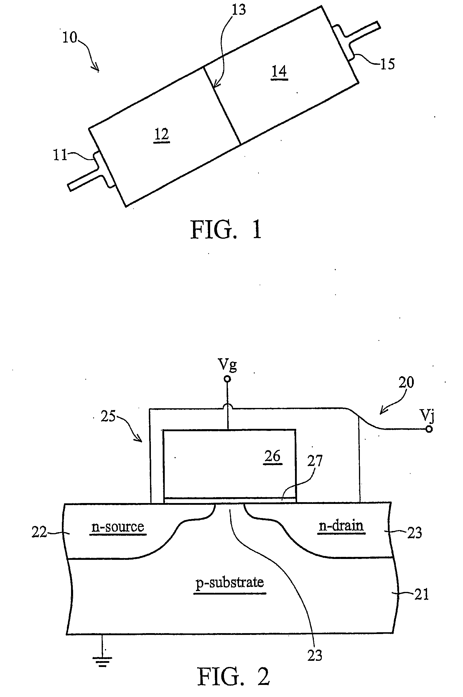
One of the more significant problems encountered with devices such as the gated diode of FIG. 2 is junction leakage.
Junction leakage is undesirable current flow, for example when in the reverse-bias or some other condition in which current flow is not supposed to occur.
Unfortunately, this can lower driving current and reduce overall device performance.
Undesirable junction capacitance is also sometimes a problem.
As should be apparent, fabricating such small devices poses many challenges.
In addition, the very short channel tends to give rise to the existence of undesirable ‘short channel effects’ (SCE), where the device does not behave in an ideal manner.

Method used


Image

  • Gated diode with non-planar source region
  • Gated diode with non-planar source region
  • Gated diode with non-planar source region

Examples


Embodiment Construction

[0026]The making and using of the presently preferred embodiments are discussed in detail below. It should be appreciated, however, that the present invention provides many applicable inventive concepts that can be embodied in a wide variety of specific contexts. The specific embodiments discussed are merely illustrative of specific ways to make and use the invention, and do not limit the scope of the invention.

[0027]The present invention provides a gated-diode or similar semiconductor device having improved SCE (short channel effect) characteristics, and a reduced junction current leakage over prior art devices. The reduction in junction leakage results in part because the device of the present invention permits a reduced electric field at a given DIBL (drain induced barrier lowering) level. Undesirable junction capacitance is also reduced. To illustrate the new features that lead to this improvement, a typical device of the prior art will first be introduced for the purposes of co...


PUM


Abstract

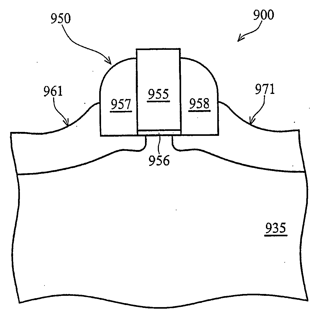
A gated-diode semiconductor device or similar component and a method of fabricating the device. The device features a gate structure disposed on a substrate over a channel and adjacent a source and a drain. The top of the source or drain region, or both, are formed so as to be at a higher elevation, in whole or in part, than the bottom of the gate structure. This configuration may be achieved by overlaying the gate structure and substrate with a profile layer that guides a subsequent etch process to create a sloped profile. The source and drain, if both are present, may be symmetrical or asymmetrical. This configuration significantly reduces dopant encroachment and, as a consequence, reduces junction leakage.

Description

TECHNICAL FIELD[0001]The present invention relates generally to semiconductor devices, and more particularly to a gated diode having a non-planar source region or source and drain region.BACKGROUND[0002]There are many types of semiconductor electronic devices. Such devices, for example diodes and transistors, take advantage of the semiconducting nature of certain materials. Because of their various advantages, they have been steadily replacing conventional electrical parts in many applications over the last half century. Some of the advantages of semiconductor devices and circuits include their low cost, small size, and generally good reliability. They are especially suited for computing and memory operations and appliances using them have become ubiquitous. Personal computers, mobile telephones, and media players are just a few examples of applications that make use of semiconductor devices.[0003]A semiconductor is a material that may be induced to act as either a conductor or as a...

Claims


Application Information

Patent Timeline
Patent Type & Authority Applications(United States)
IPC IPC(8): H01L29/78
CPCH01L29/0657H01L29/42312H01L29/66356H01L29/7391
Inventor LIN, DA-WENLIN, YING-SHIOUWANG, SHYH-WEIHUANG, LI-PINGLEUNG, YING-KEUNGDIAZ, CARLOS H.
Owner TAIWAN SEMICON MFG CO LTD
Learn More