
Methods for forming low-k dielectric films

a dielectric film and low-k technology, applied in the field of low-k dielectric film forming, can solve the problem of far fewer alternatives for k values at or below 2.6 for cvd materials, and achieve the effect of improving chemical vapor deposition

Inactive Publication Date: 2005-08-30
BOC GRP INC
View PDF8 Cites 11 Cited by
  • Summary
  • Abstract
  • Description
  • Claims
  • Application Information

AI Technical Summary

Benefits of technology

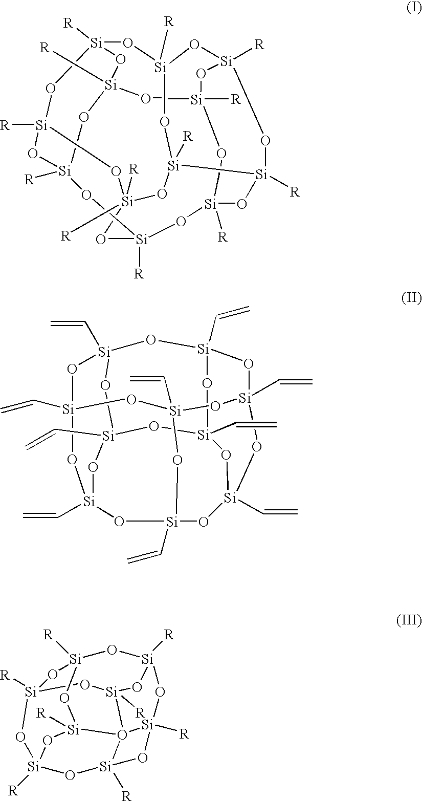
[0009]Polyhedral oligomeric silsesquioxane (POSS), having a variety of functional groups attached to a silicon oxide cage structure of the molecule, are employed in either a thermal chemical vapor deposition chamber or a plasma enhanced chemical vapor deposition chamber to form an ultra low-k dielectric film on the surface of semiconductors and integrated circuits. The POSS molecule, when combined with a linking agent in the CVD chambers, will react and polymerize to form the low-k dielectric film. The POSS molecule in general has the formula SinO1.5n (R1)i(R2)j(R3)k, n=i+j+k and can range from about 3 to about 20 wherein R1, R2, and R3 are organic or silicon functional groups or a combination of both groups.

Problems solved by technology

However, there are far fewer alternatives for k values at or below 2.6 for CVD materials in ELK / ULK applications.

Method used


Image

  • Methods for forming low-k dielectric films

Examples


examples

[0022]Two milliliters per minute of cyclohexane which contains 10% by mass of POSS #1 material, a chemical mixture of polyhedral oligometric silsesquioxane compounds containing 82% C24H36Si12O18, 16% C20H30Si10O15, and 2% C16H24Si8O12, is injected into a chamber operated at 3 torr. The solution was sprayed into the chamber using an ultrasonic nebulizer designed to deliver the solution in 20 μL droplets allowing for the complete vaporization before coming in contact with the wafer, which is heated to 250° C. In separate manifolds, methylsilane (MMS) was flowing at 100 sccm and oxygen was flowing ate 20 sccm entering into the chamber via a manifold directly above the MMS manifold. Reaction occurred on the 4″ wafer creating a 30 micron localized deposition. In comparing this to deposition on a wafer which is generated by the reaction of methylsilane, oxygen and cyclohexane in the absence of a POSS material, one fifth of the thickness of deposition occurred. This demonstrates the polyme...


PUM

PropertyMeasurementUnit
dielectric constantaaaaaaaaaa

Abstract

The use of a polyhedral oligomeric silsesquioxane compound and linking agent to form an ultra low-k dielectric film on semiconductor or integrated circuit surfaces is disclosed. The reaction between the polyhedral oligomeric silsesquioxane compound and linking agent is done in a chemical vapor deposition chamber.

Description

[0001]This application claims priority from U.S. Provisional Patent Application Ser. No. 60 / 299,409 filed Jun. 19, 2001.FIELD OF THE INVENTION[0002]The present invention provides for methods for forming a low-k dielectric film on semiconductor or integrated circuits employing a polyhedral oligomeric silsesquioxane. More particularly, the present invention provides for using the polyhedral oligomeric silsesquioxane and a polymer linking agent to form a structure that when applied as a film will have an ultra low-k dielectric constant less than or equal to 2.6.BACKGROUND OF THE INVENTION[0003]The increase in semiconductor design integration by feature size reduction has resulted in increased levels of interconnect and increased utilization of dielectric low-k thin films. The dielectric film is used as insulation around metal lines of a device and contributes to the RC time constant that controls the device speed. As the semiconductor industry has strived to reduce resistance (R) by th...

Claims


Application Information

Patent Timeline
Patent Type & Authority Patents(United States)
IPC IPC(8): C23C16/30H01L21/02H01L21/70H01L21/469H01L21/76H01L21/44H01L21/205H01L21/31H01L21/316H01L21/312C23C16/40H10B12/00
CPCC23C16/401H01L21/02126H01L21/02211H01L21/02216H01L21/02271H01L21/02274H01L21/3121H01L21/3124H01L21/02203A63B57/10G01J1/04A63B47/002A63B69/36A63B2102/32
Inventor HOGLE, RICHARD A.HELLY, PATRICK JOSEPHMA, CEMILLER, LAURA JOY
Owner BOC GRP INC
Learn More