Tunnel junctions for long-wavelength VCSELs
- Summary
- Abstract
- Description
- Claims
- Application Information
AI Technical Summary
Benefits of technology
Problems solved by technology
Method used
Image

Examples
example 1
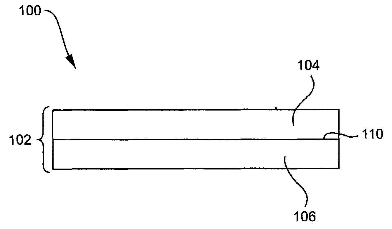
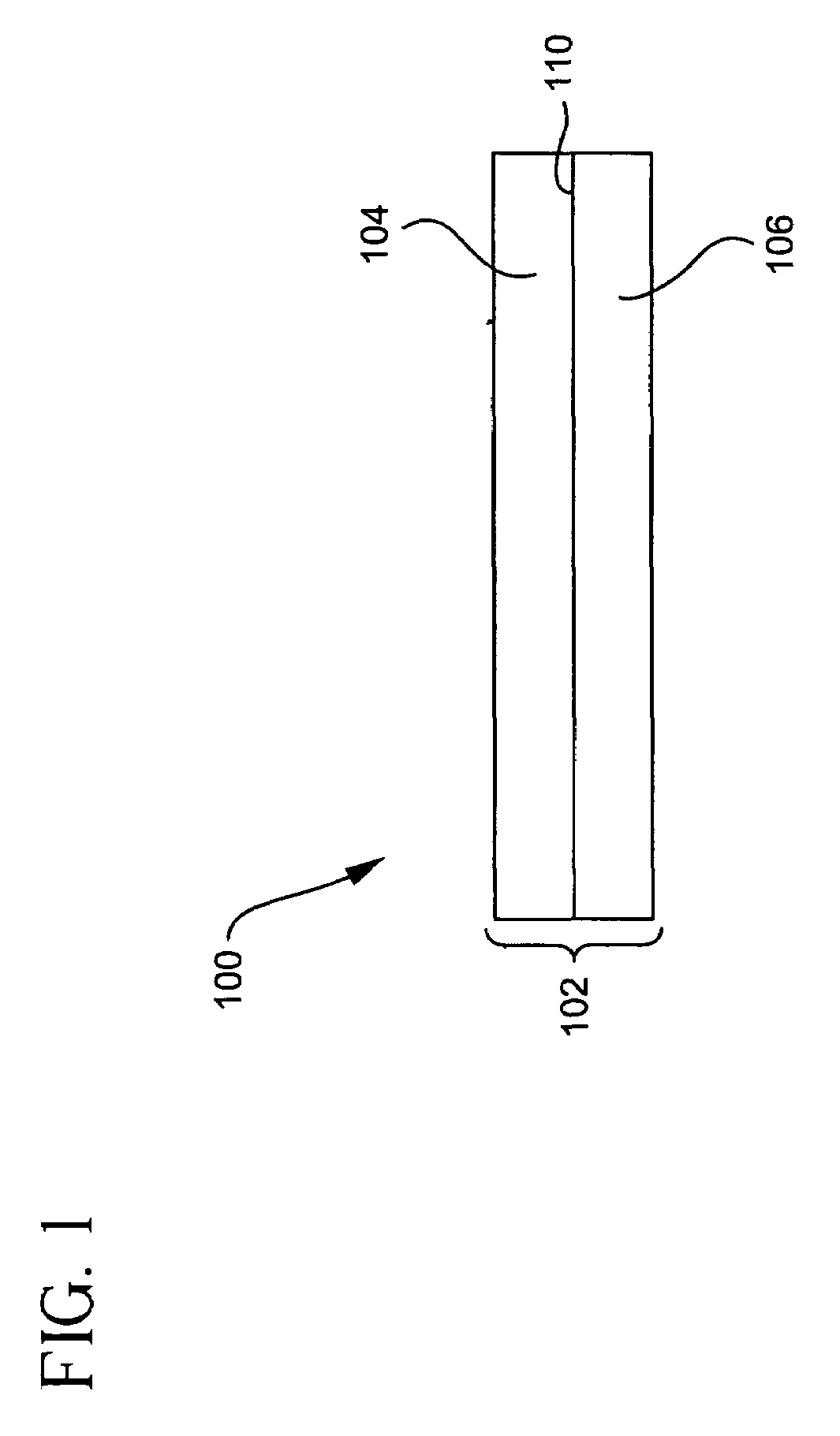
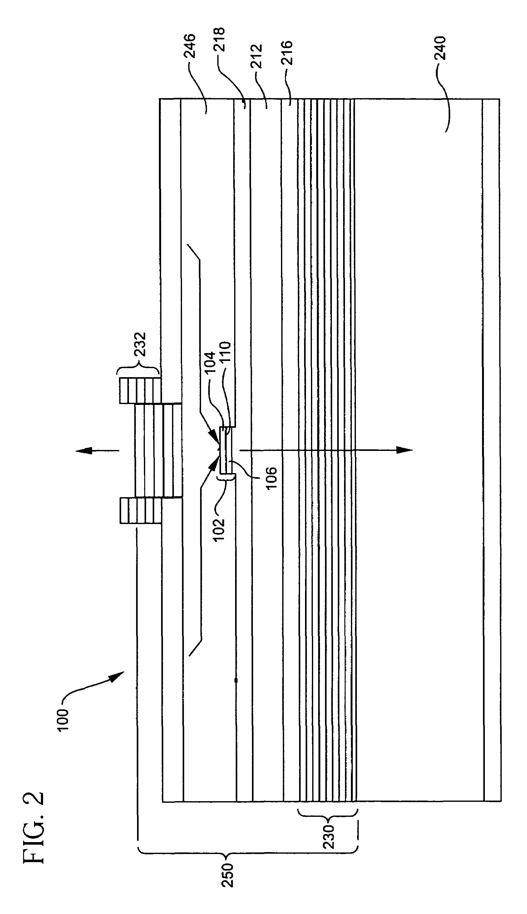
[0074]The band gap of the p-type AlGaAsSb tunnel junction layer 106 can thus be adjusted to a suitable value by adjusting the Al / Ga ratio. The p-type AlGaAsSb layer 106 and the AlGaInAs layer 104 layers may be strained. For 1.3 micron VCSELs the effective bandgap wavelengths of AlGaAsSb and AlGaInAs are selected to be 1.2 microns but other suitable values may also be used, as long as Eq. 1 is satisfied. C-doped AlGaAsSb is grown by OMCVD using suitable precursors such as trimethylaluminum, triethylgallium, arsine, trimethylantimony and carbon tetrabromide. However, any other growth method could be used. Hole concentrations of ˜3×1020 cm−3 have been achieved in AlGaAsSb. The carrier gas was hydrogen and the growth temperature was ˜550° C. A higher growth temperature is preferred in order to minimize hydrogen compensation of the C acceptors. The reagents were trimethylaluminum, triethylgallium, trimethylindium, arsine, phosphine, trimethylantimony, disilane and carbon tetrabromide. Th...
PUM
 Abstract
Description
Claims
Application Information
 - R&D
- Intellectual Property
- Life Sciences
- Materials
- Tech Scout
- Unparalleled Data Quality
- Higher Quality Content
- 60% Fewer Hallucinations
Browse by: Latest US Patents, China's latest patents, Technical Efficacy Thesaurus, Application Domain, Technology Topic, Popular Technical Reports.
© 2025 PatSnap. All rights reserved.Legal|Privacy policy|Modern Slavery Act Transparency Statement|Sitemap|About US| Contact US: help@patsnap.com