Method and apparatus to make a semiconductor chip susceptible to radiation failure

a technology of semiconductor chips and radiation failure, applied in the field of semiconductor chips, can solve the problems of limiting the performance of microprocessors, limiting the frequency increase, and large capacitance in reverse-biased junctions associated with nfet and pfet, etc., to achieve easy and broad market promotion, preserve power and performance competitive, and less radiation hard

Inactive Publication Date: 2005-06-21
MARVELL ASIA PTE LTD
View PDF2 Cites 25 Cited by
  • Summary
  • Abstract
  • Description
  • Claims
  • Application Information

AI Technical Summary

Benefits of technology

[0033]The present invention is a method and apparatus that preserves the power and performance competitive advantages of SOI CMOS or similar radiation-hard semiconductor products, but which is less radiation-hard and therefore can be more easily and more broadly marketed.

Problems solved by technology

Several limitations of bulk CMOS are beginning to limit continued increases in frequencies.
A first limitation of bulk CMOS is the relatively large amount of capacitance in the reverse-biased junctions associated with NFET and PFET drains.
Thus the capacitance of the drains of the NFETs and PFETs limit the performance of the microprocessor or the ASIC.
In these circuits, the sources of most of the Field Effect Transistors (FETs) in the stacks of NFETs and PFETs also often are switched from one voltage level to another, further adding to capacitance that must be switched, and thus degrading performance.
Undesired capacitance not only degrades performance, but also causes more power to be dissipated.
Power is becoming a serious problem.
Even when large computers or other electronic products are plugged into the wall, heat buildup calls for elaborate and expensive cooling mechanisms.
A second limitation of bulk CMOS is that the bodies of all NFETs are coupled to ground (or another suitable lower voltage).
Creation of semiconductor chips involves relatively high fixed costs.
The products have to be designed, requiring expensive design tools and engineering labor.
In addition, the fabrication of the products requires extremely expensive semiconductor tools and factories.
These failures are often called soft errors.
The United States government restricts foreign sale or export of such products to some countries.
SOI CMOS microprocessors, Static Random Access Memories (SRAMs), Dynamic Random Access Memories (DRAMs), and ASIC products are resistant enough to radiation to fall into the radiation-hardened microelectronic circuit category, and are therefore subject to export restrictions and market limitations.
Semiconductor products produced on such processes also have their markets limited by the United States Government munitions restrictions.

Method used


Image

  • Method and apparatus to make a semiconductor chip susceptible to radiation failure
  • Method and apparatus to make a semiconductor chip susceptible to radiation failure
  • Method and apparatus to make a semiconductor chip susceptible to radiation failure

Examples


Embodiment Construction

[0054]Having reference now to the figures, the present invention will be described in detail.

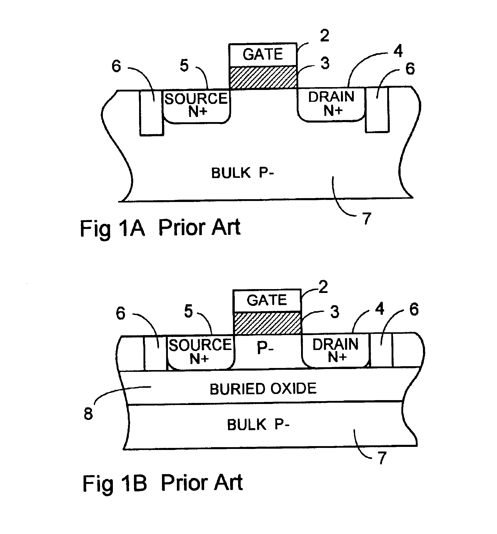
[0055]FIG. 1A shows a cross section of a conventional N-channel Field Effect Transistor (NFET), comprising a gate 2, a gate oxide 3, a drain 4, a source 5, and shallow trench isolation 6, constructed in a bulk P− silicon substrate. Such a structure is sensitive to radiation. A high-energy particle (not shown) will ionize a region in the bulk P− substrate 7. Positive charges will be drawn off to a low voltage supply (usually ground) to which the substrate is coupled. Negative charges will be attracted to a positively charged drain 4. In precharged circuits, such as Dynamic Random Access Memory (DRAM) precharged logic, or in high-impedance circuits such Static Random Access Memory (SRAM), the accumulation of the negative charges on a positively-charged N+ drain, can cause faulty operation. Similarly, accumulation of positive charges on a negatively precharged P+ drain can cause faulty operatio...


PUM


Abstract

Methods and apparatus are provided for reducing the overall radiation hardness of a semiconductor chip. A radiation detector and a failure memory are provided. A disable signal or signals is produced by the failure memory. The disable signal is a required input to a user logic function, such as an off chip driver, an off chip receiver, a clock, or a static random access memory. When the radiation detector detects radiation, that detection is stored in the failure memory. The disable signal, when active, causes some or all of the user function to be inoperative. This invention is particularly important when the semiconductor chip is produced in a silicon on insulator (SOI) Complementary Metal Oxide Semiconductor (CMOS) process, which is naturally radiation resistant.

Description

FIELD OF THE INVENTION[0001]The present invention relates to semiconductor chips. In particular, the present invention relates reducing radiation hardness on chipsDESCRIPTION OF THE RELATED ART[0002]Very Large Scale Integration (VLSI) employing bulk substrate Complementary Metal Oxide Semiconductor (CMOS) technology has been one of the major success stories in recent years. Virtually all of the recent high performance microprocessors, as well as the Application Specific Integrated Circuit (ASIC) chips have been implemented in CMOS on a bulk substrate.[0003]Bulk substrate technology provides a relatively inexpensive foundation upon which to create the N-channel Field Effect Transistors (NFETs) and the P-channel Field Effect Transistors (PFETs) needed to make modern logic circuits, such as NANDs, NORs, and memory elements, such as latches, registers, and Static Random Access Memories (SRAMs). CMOS implemented on a bulk substrate technology is called bulk CMOS. Source and drain areas o...

Claims


Application Information

Patent Timeline
IPC IPC(8): G11C11/412H01L21/762H01L21/70H01L27/12H03K19/173
CPCG11C11/4125H03K19/1731H01L27/1203H01L21/76243
Inventor FRIEND, DAVID MICHAELVAN PHAN, NGHIAROHN, MICHAEL JAMES
Owner MARVELL ASIA PTE LTD
Why Eureka
Try Eureka