
Tab package

a packaging structure and tab technology, applied in the direction of electrical apparatus construction details, casings/cabinets/drawers, casings/cabinets/drawers details, etc., can solve the problems of increasing the overall circuit length, complicated structure, and low heat dissipation capacity of this type of package, so as to reduce the overall thickness of the package and improve the electrical performance , the effect of short circuit path

Inactive Publication Date: 2005-05-17
VIA TECH INC
View PDF6 Cites 15 Cited by
  • Summary
  • Abstract
  • Description
  • Claims
  • Application Information

AI Technical Summary

Benefits of technology

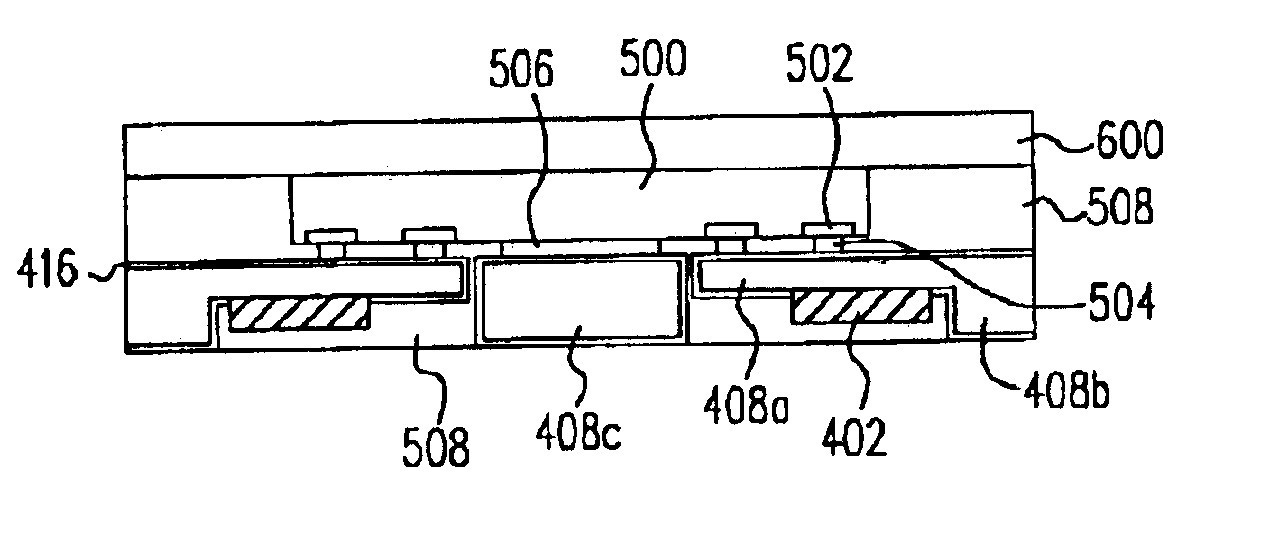
The present invention provides a TAB package structure and a corresponding fabrication method that can reduce overall thickness of the package and improve electrical performance. The TAB package structure includes a tape carrier, a chip, a plurality of electrical contacts, and a heat sink. The tape carrier has a device opening and a plurality of outer lead openings. The chip is placed on the tape carrier and a thermal compression process is carried out to encapsulate the chip and form an integrative unit. The TAB package structure also includes a second heat sink attached to the backside of the chip. The invention also provides a method of fabricating a tape carrier and a method of fabricating a TAB package structure.

Problems solved by technology

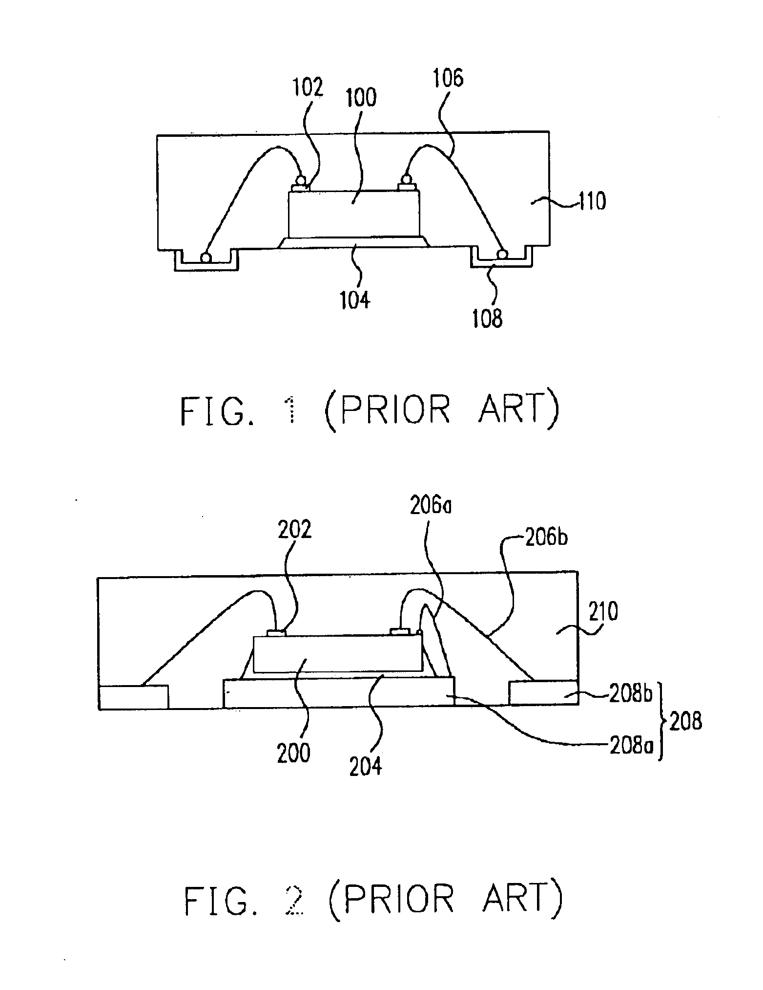
Hence, the structure is a bit complicated to fabricate.
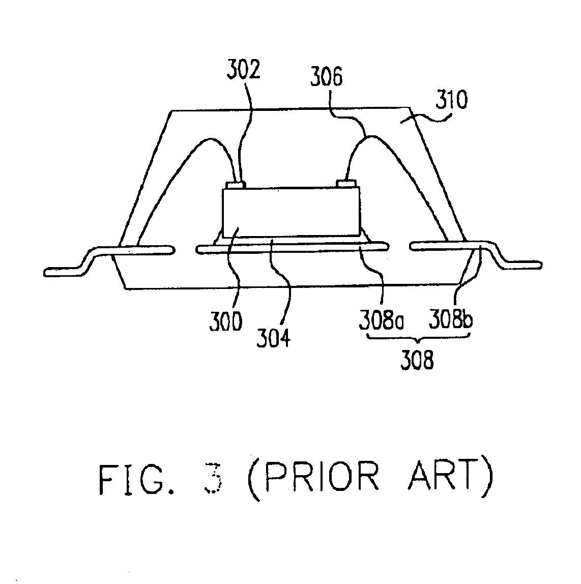
Consequently, heat dissipation capacity for this type of package is usually low.
After the redistribution process, overall circuit length will be increased so that parasitic inductance problem may crop up.

Method used


Image

  • Tab package
  • Tab package
  • Tab package

Examples


first embodiment

[0032]FIGS. 4A to 4F are schematic cross-sectional views showing the progression of steps for fabricating a tape automated bonding package according to this invention. First, as shown in FIG. 4A, a conductive layer 408 having a plurality of bumps thereon is provided. The conductive layer 408 is a metallic layer such as a copper layer. The bumps on the conductive layer 408 are formed, for example, by half-etching.

[0033]A tape 402 made from polyimide material, for example, is provided as shown in FIG. 4B. The tape 402 is attached to the conductive layer 408. The tape 402 has a plurality of openings 404 and a device opening 406 thereon. The device opening 406 is located in the middle of the tape 402 and the openings 404 are positioned around the device opening 406, for example. After placing the tape 402 under the conductive layer 408, the bumps on the conductive layer 408 will pass through the openings 404 and the device opening 406.

[0034]As shown in FIG. 4C, a resin layer 414 is form...

second embodiment

[0038]FIGS. 5A to 5G are schematic cross-sectional views showing the progression of steps for fabricating a tape automated bonding package according to this invention. As shown in FIG. 5A, a tape 702 having a plurality of openings 704 and a device opening 702 thereon is provided. The device opening 706 is located in the middle of the tape 702 while the openings 704 are positioned around the device opening 706. The tape 702 is typically made, for example, from a polyimide material.

[0039]As shown in FIG. 5B, a conductive layer 708 is provided. The conductive layer 708 is attached to the tape 702. In this embodiment, the conductive layer 708 is a slab of conductive material such as copper with planar surfaces.

[0040]As shown in FIG. 5C, a resin layer 714 is formed over the tape 702. Thereafter, a portion of the conductive layer 708 is removed to form leads each having an inner lead section 708a and an outer lead section 708b and a heat sink 708c. The conductive layer 708 is patterned, f...


PUM


Abstract

A tape automated bonding (TAB) package and a method for fabricating the same is provided. A chip (a wire-bond chip or a flip chip) is bonded to a tape carrier through thermal compression. The chip and the tape carrier are encapsulated inside a molding compound. To enhance the TAB package thermally, a heat sink is attached to the backside of the chip.

Description

CROSS REFERENCE TO RELATED APPLICATIONS[0001]This application claims the priority benefit of Taiwan application serial no. 91120048, filed Sep. 3, 2002.BACKGROUND OF INVENTION[0002]1. Field of Invention[0003]The present invention relates to a tape automated bonding (TAB) packaging structure and method of fabricating the same. More particularly, the present invention relates to a TAB packaging structure having a heat sink thereon and a method of fabricating the same.[0004]2. Description of Related Art[0005]In this information consciousness society, multi-media applications are being developed at a tremendous pace. To keep up with this trend, integrated circuit packages inside electronic devices must match a set of corresponding demands for digital input, networking, local area connection and personalized usage. In other words, each electronic device must be highly integrated so that more powerful programs can be executed at a higher speed and yet each package has to occupy less space...

Claims


Application Information

Patent Timeline
Patent Type & Authority Patents(United States)
IPC IPC(8): H01L23/367H01L23/498H01L23/34H01L23/48
CPCH01L23/3677H01L23/4985H01L2924/10253H01L2224/73265H01L2224/48247H01L2224/32245H01L24/48H01L2224/16H01L2224/48237H01L2924/01079H01L2924/30107H01L2924/3025H01L2924/00H01L2924/00015H01L2924/14H01L2224/05571H01L2224/05573H01L2924/00014H01L2924/181H01L2924/18165H01L2224/48257H01L2924/1815H01L2224/45099H01L2224/05599H01L2224/85399H01L2924/00012H01L2224/45015H01L2924/207
Inventor KUNG, MORISSHO, KWUN-YAO
Owner VIA TECH INC
Learn More