
Apparatus and method for fabrication of photonic crystals

a photonic crystal and apparatus technology, applied in the direction of crystal growth process, gel state, instruments, etc., can solve the problems of high cost, difficult to fabricate a very large size single crystal, etc., to achieve the effect of reducing cos

Inactive Publication Date: 2005-05-17
UNIV OF CONNECTICUT
View PDF6 Cites 22 Cited by
  • Summary
  • Abstract
  • Description
  • Claims
  • Application Information

AI Technical Summary

Benefits of technology

The present invention provides an improved fabrication process for creating photonic crystals that are comparable in size and complexity to those made using microlithographic techniques, but at a significantly reduced cost. These crystals can be used in various applications such as opto-electronic and photonic devices. The invention also provides a system for fabricating photonic crystals using a evanescent light interference pattern grid and a method for introducing controlled local variations into photonic crystals. Overall, the invention offers a more efficient and flexible way to create photonic crystals.

Problems solved by technology

E-beam lithography / reactive ion etching suffers from fabrication complexity.
Beyond the problem of generating a complete photonic band gap in a synthetic opal formed by self-ordering of submicron colloidal spheres made either from polymers or silica, one of the biggest limitations associated with this approach is the fact that it is extremely difficult to fabricate a very large size single crystal.
In practice, nucleation sites having different crystal orientations (such as illustrated in FIGS. 8A and 8B) have limited technological applications.
Although the recent interest in photonic 3D periodic crystals that exhibit periodic modulation in refractive index has caused significant excitement in the scientific community, commercial realization of such well-controlled periodic structures, in particular where well-defined defects are inserted within, has been elusive.
That is, the creation of long-range 3D single crystals with controlled-defects, in a manner that can be mass-produced, is not presently available for most materials.
The methods set forth above for manufacturing phototonic crystals are simply too laborious and are limited to a restricted number of materials which can be employed in the construction process.
No economically viable alternative approaches have been reported.

Method used


Image

  • Apparatus and method for fabrication of photonic crystals
  • Apparatus and method for fabrication of photonic crystals
  • Apparatus and method for fabrication of photonic crystals

Examples


Embodiment Construction

[0042]The present invention defines a process (and the crystal produced thereby) wherein the self-ordering of submicron “monodispersed” (narrow dispersion of sizes) spheres are assembled with the assistance of an optically defined lattice capable of maintaining a single crystal orientation over substantial distances. The invention permits photonic crystals to be fabricated from a wider variety of materials than possible under the prior art and permits single photonic crystals to be formed in a size larger than available under the prior art. The process for forming photonic crystals of the present invention also proffers the ability to produce photonic crystals at significantly lower expense than prior art processes.

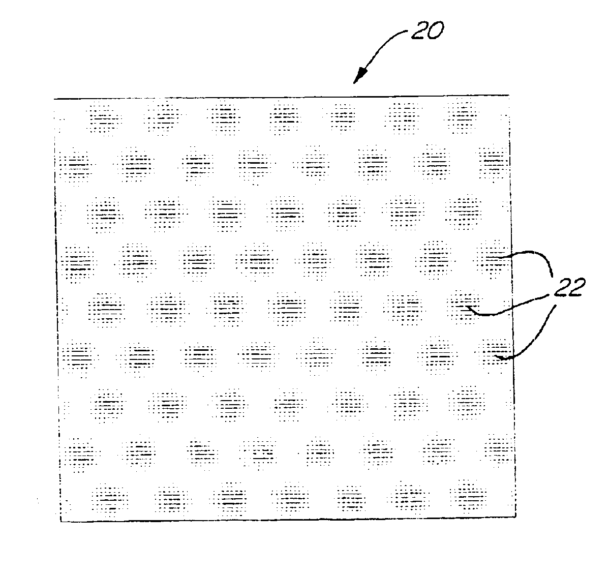
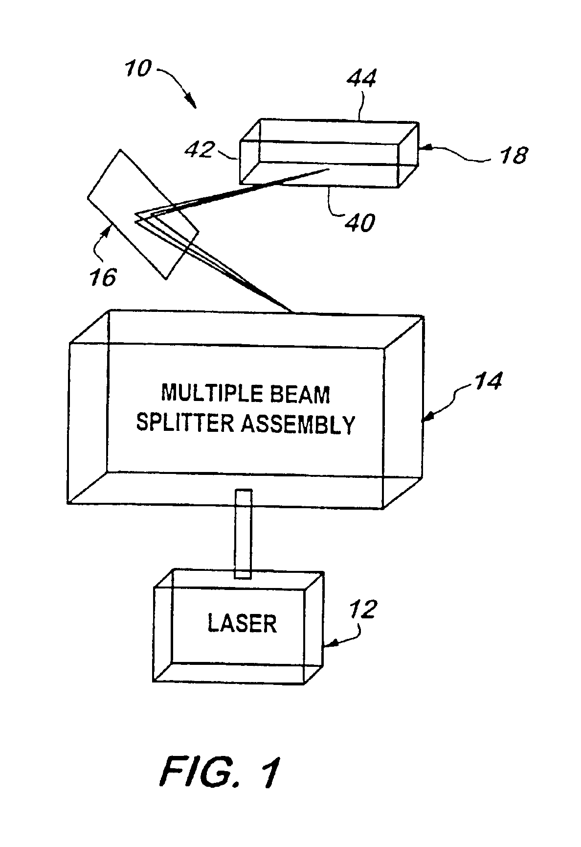
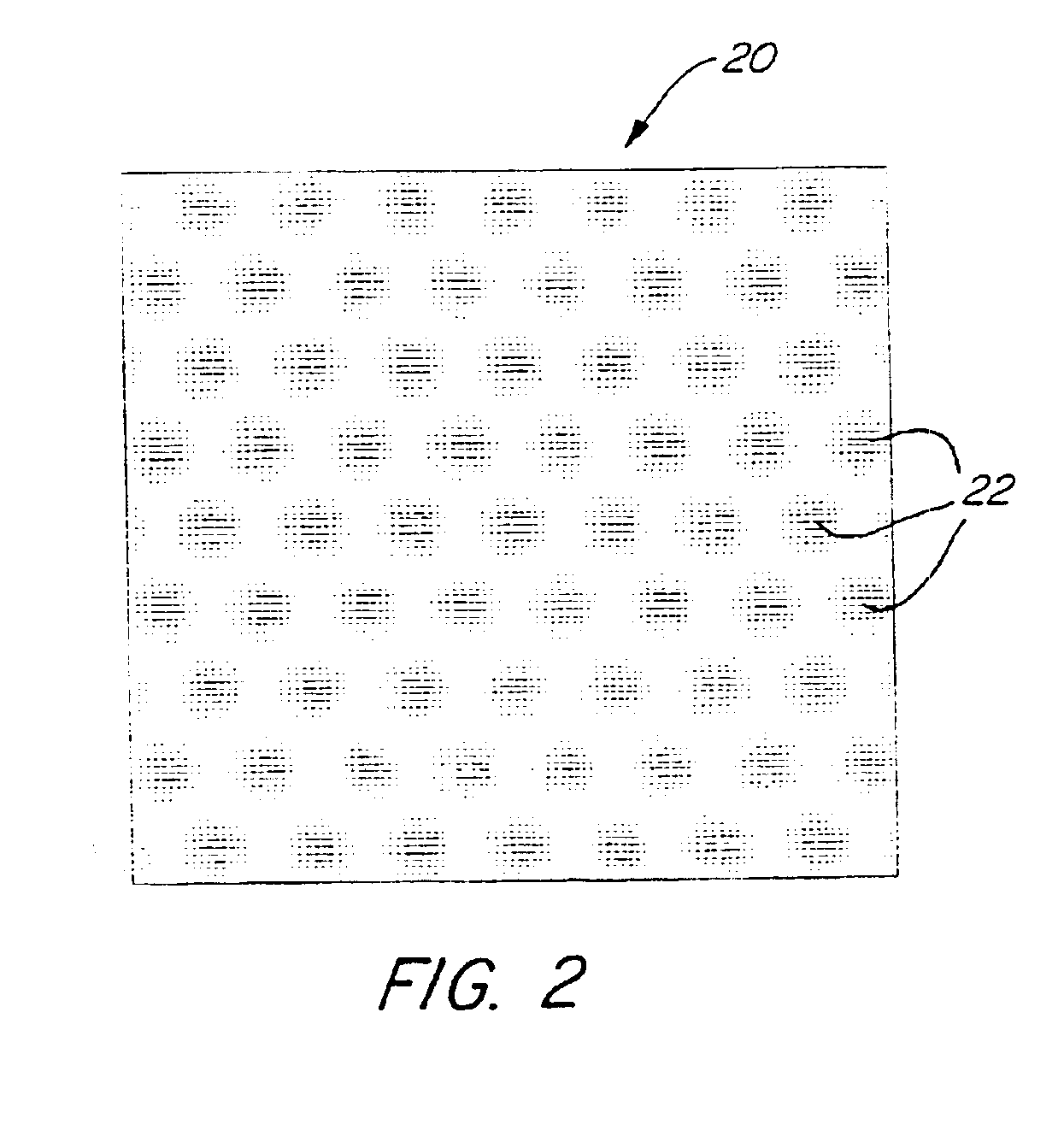
[0043]In FIGS. 1 and 3, one embodiment of the photonic crystal fabrication apparatus of the present invention is indicated generally by the reference numeral 10. The photonic crystal fabrication apparatus 10 comprises a LASER or other coherent light source 12, a multiple ...


PUM

PropertyMeasurementUnit
relative interference angleaaaaaaaaaa
interplanar distanceaaaaaaaaaa

Abstract

A process for the fabrication of a photonic crystal (and the crystal produced thereby) comprising producing a first beam of coherent light; generating a second and a third beam of coherent light each in a fixed phase relationship with the first beam; aligning the beams of coherent light so as to form a fixed relative angle of incidence between each pair of beams and to form an evanescent light interference pattern grid on a substrate having a first electrostatic charge; introducing into the evanescent light interference pattern grid a substance having a second electrostatic charge of an attractive nature to the first electrostatic charge; positioning the substance with the second electrostatic charge using the evanescent interference pattern grid in a planned manner on the substrate so as to form a photonic crystal. An apparatus for fabricating a photonic crystal is provided comprising a sample cell having a first electrostatic surface charge; a coherent light source operatively configured to generate a first beam of coherent light; at least one beam splitter optically coupled to the coherent light source for generating at least a second and a third beam of coherent light from the first beam of coherent light; at least one reflector in alignment with the beam splitter so as to receive the first, second and third beams of coherent light, said reflector operatively configured to align said first, second and third beams so as to form a relative angle of incidence between each pair of beams of approximately 120 degrees and to form an evanescent light interference pattern grid on said sample cell; which pattern gild can be used to position particles of a second electrostatic surface charge on the sample cell.

Description

FIELD OF THE INVENTION[0001]The present invention relates to photonic crystal fabrication, and more particularly, to laser-assisted solid freeform fabrication of photonic crystals, in particular of the micro and / or meso type.BACKGROUND INFORMATION[0002]In recent years, there has been a growing interest in developing micro / meso photonic structures with well-controlled periodic structures and well-defined defects. In particular there has been growing interest in the fabrication of photonic crystals. Photonic crystals (also known as photonic band-gap materials) are periodic dielectric structures that have a band gap that forbids propagation of a certain frequency of light. In photonic crystals three-dimensional (3D) periodic modulation in refractive index is used to cause an incident electromagnetic (EM) radiation with wavelength proportional to the periodicity of the photonic crystal to undergo Bragg diffraction in a given direction, resulting in the formation of a stop band in the tr...

Claims


Application Information

Patent Timeline
Patent Type & Authority Patents(United States)
IPC IPC(8): C30B35/00C30B5/00G02B6/122
CPCB82Y20/00C30B5/00G02B6/1225C30B35/00C30B29/68
Inventor PAPADIMITRAKOPOULOS, FOTIOSMARCUS, HARRIS L.
Owner UNIV OF CONNECTICUT
Learn More