
Nondestructive characterization of thin films based on acquired spectrum

a spectrum acquisition and characterization technology, applied in the field of solid sample characterization, can solve the problems of insufficient depth profiling techniques, difficult characterization of thin films, and insufficient speed of characterization, so as to improve precision, less precise, and enhance data quality

Inactive Publication Date: 2005-05-10
NOVA MEASURING INSTRUMENTS INC
View PDF17 Cites 58 Cited by
  • Summary
  • Abstract
  • Description
  • Claims
  • Application Information

AI Technical Summary

Benefits of technology

[0019]The present invention may employ novel data reduction that includes, for example, a fitting process to compare measured peak shapes for elemental and / or chemical species (e.g., Si peak shapes previously measured for a particular process to be monitored) to collected XPS data, e.g., using a non-linear least squares fitting algorithm. Such fitting is performed without the necessary conventional operator input. In such a manner, e.g., with elimination of frequent operator input that conventionally made the results operator dependent and less precise, enhancement of the data quality yielding improved precision is accomplished.

Problems solved by technology

Such thin films are difficult to characterize.
Further, such techniques may also require the characterization to be performed with ample speed.
However, in process monitoring, such depth profiling techniques are in many circumstances inadequate.
For example, depth profiling is an invasive and destructive process, and further, such processes generally take a relatively long period of time to complete, e.g., as compared to just surface measurements.
Further, even if such techniques are not used in a destructive depth profiling fashion, they are typically inadequate in many other respects with regard to characterization of various types of samples.
Since nitrogen content varies with depth, the index of refraction of the films is a variable making it difficult to use standard optical methods to monitor SiON films.
. . ) is challenging the fundamental limits of optical methods.
The combination of these two effects has reduced measurement precision for thickness using such techniques rendering them ineffective for monitoring thickness and composition.
However, there are a number of issues that make the TEM impractical for use in production monitoring.
For example, thickness measurement precision is typically greater than 2 angstroms and the cost of the needed equipment is generally prohibitive.
Further, the length of time needed to perform such measurements is long (e.g., four hours per measurement) and a highly skilled specialist to prepare the sample and perform the measurements is typically a requirement.
However, the high intensity electron beam used to make Auger measurements can alter the apparent composition of a thin film by causing chemical damage (e.g., can damage SiO2 films) or causing the migration of elements within the thin film.
Use of a low analyzer angle generally results in a slow characterization process and also may result in problems associated with placement of the analyzer of the characterization system relative to the sample being analyzed.
Yet further, existing data reduction methods which operate on the XPS collected data employ software tools for background subtraction and peak fitting that require frequent operator input making the results operator dependent and less precise.
Such techniques, e.g., those that use removal of material during depth profiling, are sufficient in many circumstances, e.g., research and development, product testing, etc., but do not provide for the ability to quickly analyze a thin film such as is necessary in production processes.
Such gate structures are only one of the growing number of semiconductor related material structures under development that require characterization at an unprecedented level of complexity.

Method used


Image

  • Nondestructive characterization of thin films based on acquired spectrum
  • Nondestructive characterization of thin films based on acquired spectrum
  • Nondestructive characterization of thin films based on acquired spectrum

Examples


Embodiment Construction

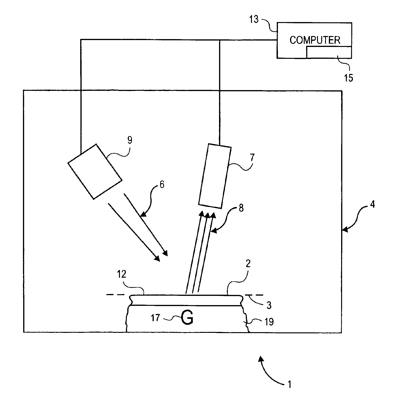
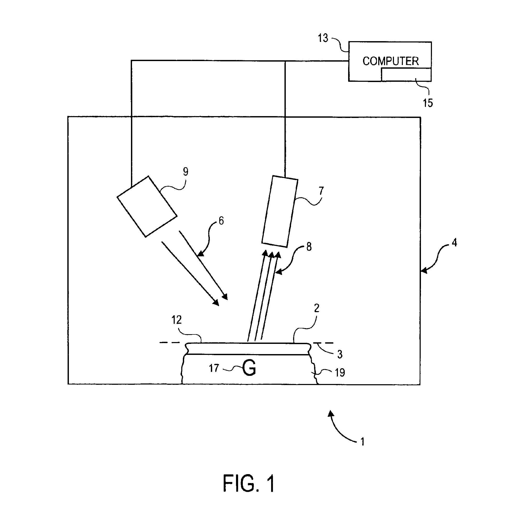
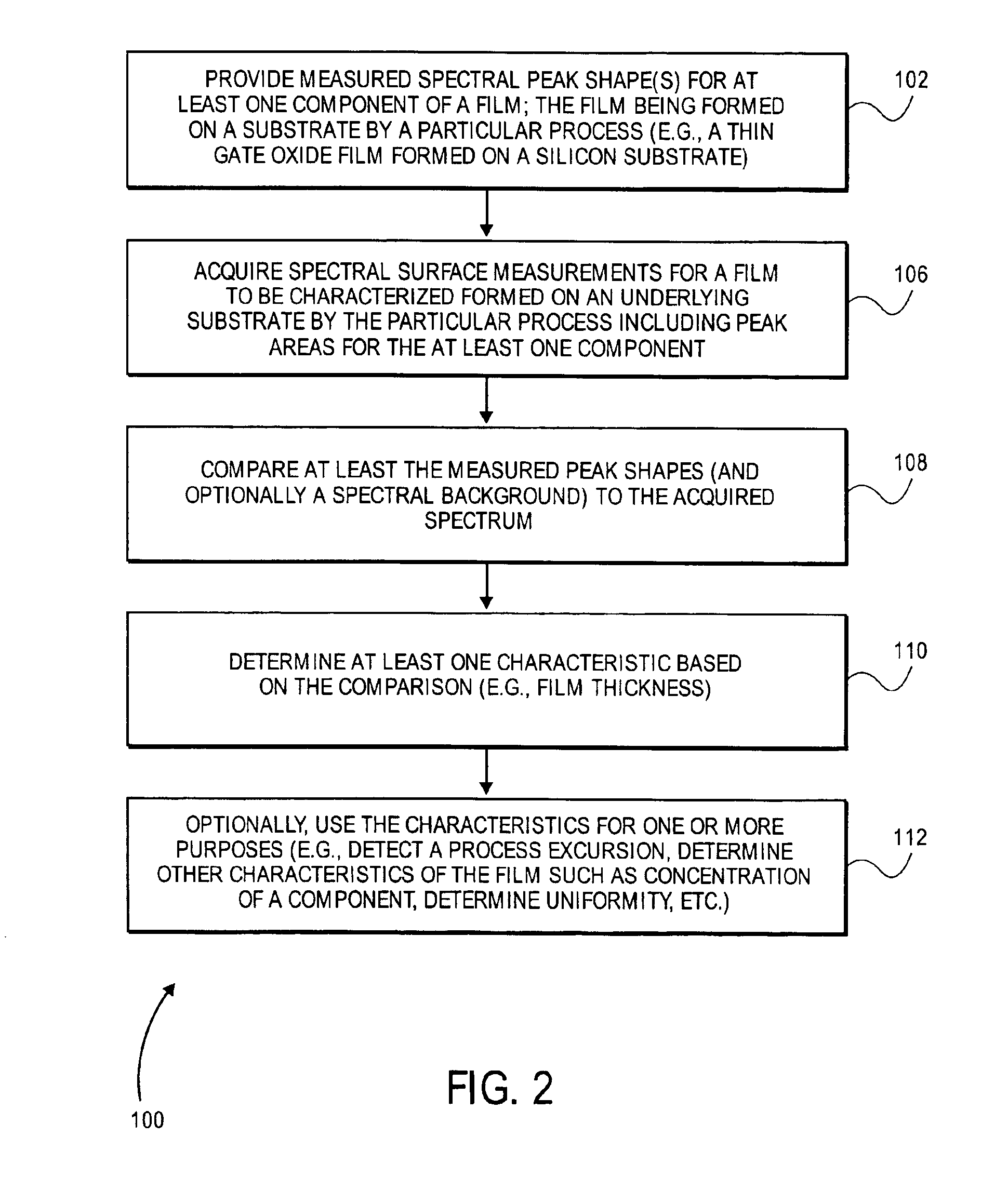
[0046]Analysis systems and methods according to the present invention shall be described with reference to FIGS. 1-15. Such systems and methods may be used to analyze complex materials in development processes, assist to identify solutions for processing problems, identify contamination sources, improve yields in the fabrication of devices, assist in monitoring processing and manufacturing devices, and be used in failure analysis techniques. Further, the systems and methods may be used in the characterization of thin films relating to various industrial applications, such as semiconductor devices, magnetic storage media, display technology, automotive materials, aerospace materials, polymer products, and / or biomaterials.

[0047]Generally, the analysis systems and methods described herein preferably provide non-destructive, e.g., non-invasive, analysis systems and methods that generally include the collection of surface spectral measurements (e.g., XPS spectra) from a thin film. Therea...


PUM


Abstract

The present invention provides for characterization of a film (e.g., thickness determination for a silicon oxynitride film) using collected spectral data. For example, an acquired spectrum may be cumulatively integrated and the geometric properties of the integrated spectrum may be used to determine component concentration information. Thickness measurements for the film may be provided based on the component concentration information.

Description

FIELD OF THE INVENTION[0001]The present invention relates to the characterization of solid samples, e.g., thin films. More particularly, the present invention pertains to the use of nondestructive techniques to characterize such samples.BACKGROUND OF THE INVENTION[0002]Characterization or analysis of samples (e.g., thickness of a thin film, elemental and / or chemical species concentration in a thin film formed on a substrate, etc.) is necessary in the manufacture of many different types of devices (e.g., electronic and optical electronic devices). For example, it may be necessary to determine the composition of thin dielectric films (e.g., gate oxide films, tantalum nitride films, etc.) formed in known semiconductor integrated circuit devices, such as processing devices and memory devices. Increases in the density of such devices on an integrated circuit chip and reduction in device dimensions require the advancement of production processes and characterization technologies related t...

Claims


Application Information

Patent Timeline
IPC IPC(8): G01B15/02
CPCG01B15/02
Inventor LARSON, PAUL E.WATSON, DAVID G.
Owner NOVA MEASURING INSTRUMENTS INC
Learn More