Liquid crystal display device
a liquid crystal display and liquid crystal technology, applied in the direction of identification means, instruments, optics, etc., can solve the problems of remarkable visual dependence, low response speed of liquid crystal display devices using nematic liquid crystals, and inability to adapt to the display of moving images
- Summary
- Abstract
- Description
- Claims
- Application Information
AI Technical Summary
Benefits of technology
Problems solved by technology
Method used
Image
Examples
second embodiment
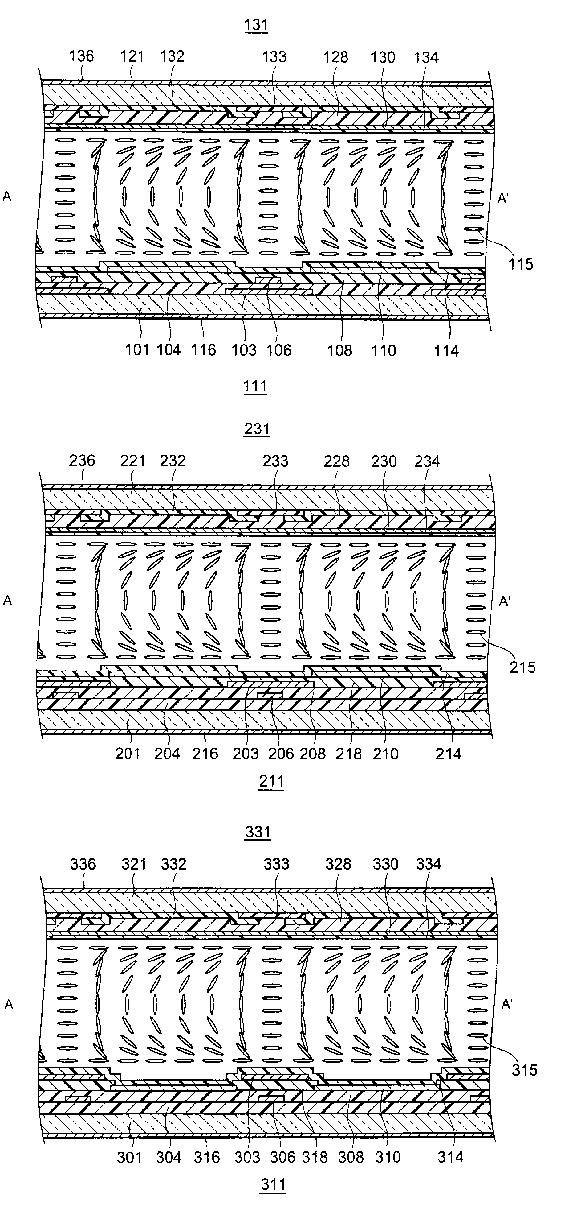
Subsequently, a method of manufacturing the liquid crystal display device of the second embodiment will be described with reference to FIGS. 3 and 5.
An aluminum film is deposited on a glass substrate 201 by a sputtering method and a scan signal electrode 202 is formed by a photolithography technique. A gate insulating film 204 is formed on the scan signal electrode 202 and an amorphous silicon film is formed on the gate insulating film 204 by a chemical evaporation method, and then, impurity ions are implanted thereinto. After that, a semiconductor island 205 made of amorphous silicon is formed by a photolithography technique to constitute an active layer of a thin film transistor corresponding to each pixel. A chromium film is deposited on the semiconductor island 205 by a sputtering method, and a video signal electrode (=source electrode) 206 and a drain electrode 207 are formed by a photolithography technique. A first interlayer insulating film 208 made from a silicon oxide film ...
third embodiment
Subsequently, a method of manufacturing the liquid crystal display device of the third embodiment will be described with reference to FIGS. 3 and 6.
An aluminum film is deposited on a glass substrate 301 by a sputtering method and a scan signal electrode 302 is formed by a photolithography technique. A gate insulating film 304 is formed on the scan signal electrode 302 and an amorphous silicon film is formed on the gate insulating film 304 by a chemical evaporation method, and then, impurity ions are implanted thereinto. After that, a semiconductor island 305 made of amorphous silicon is formed by a photolithography technique to constitute an active layer of a thin film transistor corresponding to each pixel. A chromium film is deposited on the semiconductor island 305 by a sputtering method and a video signal electrode (=source electrode) 306 and a drain electrode 307 are formed by a photolithography technique. A first interlayer insulating film 308 made from a silicon oxide film is...
seventh embodiment
Subsequently, a method of manufacturing a liquid crystal display device of the seventh embodiment will be described with reference to FIGS. 11 and 12.
An aluminum film is deposited on a glass substrate 701 by a sputtering method and a scan signal electrode 702 is formed by a photolithography technique. A gate insulating film 704 is formed on the scan signal electrode 702 and an amorphous silicon film is formed on the gate insulating film 704 by a chemical evaporation method, and then, impurity ions are implanted thereinto. After that, the semiconductor island 705 made of amorphous silicon is formed by a photolithography technique to form an active layer of a thin film transistor in each pixel. A chromium film is deposited on the semiconductor island 705 by a sputtering method, and a video signal electrode (=source electrode) 706 and a drain electrode 707 are formed by a photolithography technique. A first interlayer insulating film 708 made from a silicon oxide film is formed on the ...
PUM
| Property | Measurement | Unit |
|---|---|---|
| response time | aaaaa | aaaaa |
| voltage | aaaaa | aaaaa |
| voltage | aaaaa | aaaaa |
Abstract
Description
Claims
Application Information
 - R&D
- Intellectual Property
- Life Sciences
- Materials
- Tech Scout
- Unparalleled Data Quality
- Higher Quality Content
- 60% Fewer Hallucinations
Browse by: Latest US Patents, China's latest patents, Technical Efficacy Thesaurus, Application Domain, Technology Topic, Popular Technical Reports.
© 2025 PatSnap. All rights reserved.Legal|Privacy policy|Modern Slavery Act Transparency Statement|Sitemap|About US| Contact US: help@patsnap.com


