
Optical amplifier

a technology of optical amplifier and optical fiber, applied in the direction of electromagnetic transmission, semiconductor laser, active medium material, etc., can solve the problems of abrupt decrease very different gain in the er-doped optical fiber at different wavelengths, and the referred device of conventional non-temperature-regulated excitation light source, etc., to achieve the effect of sufficiently small wavelength dependence of gain in the er-doped optical fiber

Inactive Publication Date: 2005-03-22
SUMITOMO ELECTRIC IND LTD
View PDF18 Cites 4 Cited by
  • Summary
  • Abstract
  • Description
  • Claims
  • Application Information

AI Technical Summary

Benefits of technology

An object of the present invention is to provide an optical amplifier wherein the wavelength dependence of gain in the Er-doped optical fiber can be made sufficiently small.
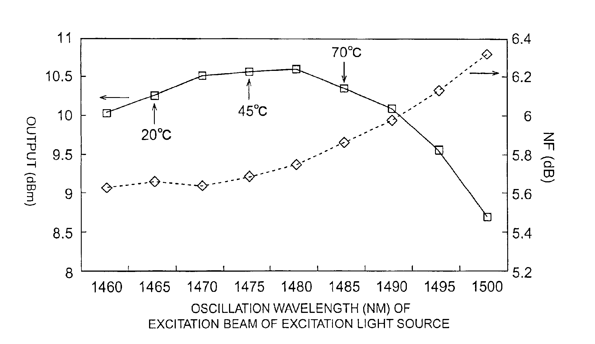
As a result of meticulous study aimed at solving the above problem, the present inventors discovered that the above problem could be solved by employing a semiconductor laser element wherein the oscillation wavelength at 20° C. is less than 1470 nm but not less than 1440 nm in a so-called non-temperature regulated excitation light source device, and thereby perfected the present invention.

Problems solved by technology

However, the conventional non-temperature regulated excitation light source device referred to above has the following problems.
Specifically, in a non-temperature regulated excitation light source device, when the temperature of the semiconductor laser element becomes high, the oscillation wavelength of the semiconductor laser element shifts into a wavelength region longer than 1480 nm; however, when the oscillation wavelength becomes longer than 1480 nm, the gain in the Er-doped optical fiber abruptly decreases, so there was the problem that the gain in the Er-doped optical fiber was very different at different wavelengths.

Method used


Image

  • Optical amplifier
  • Optical amplifier
  • Optical amplifier

Examples


Embodiment Construction

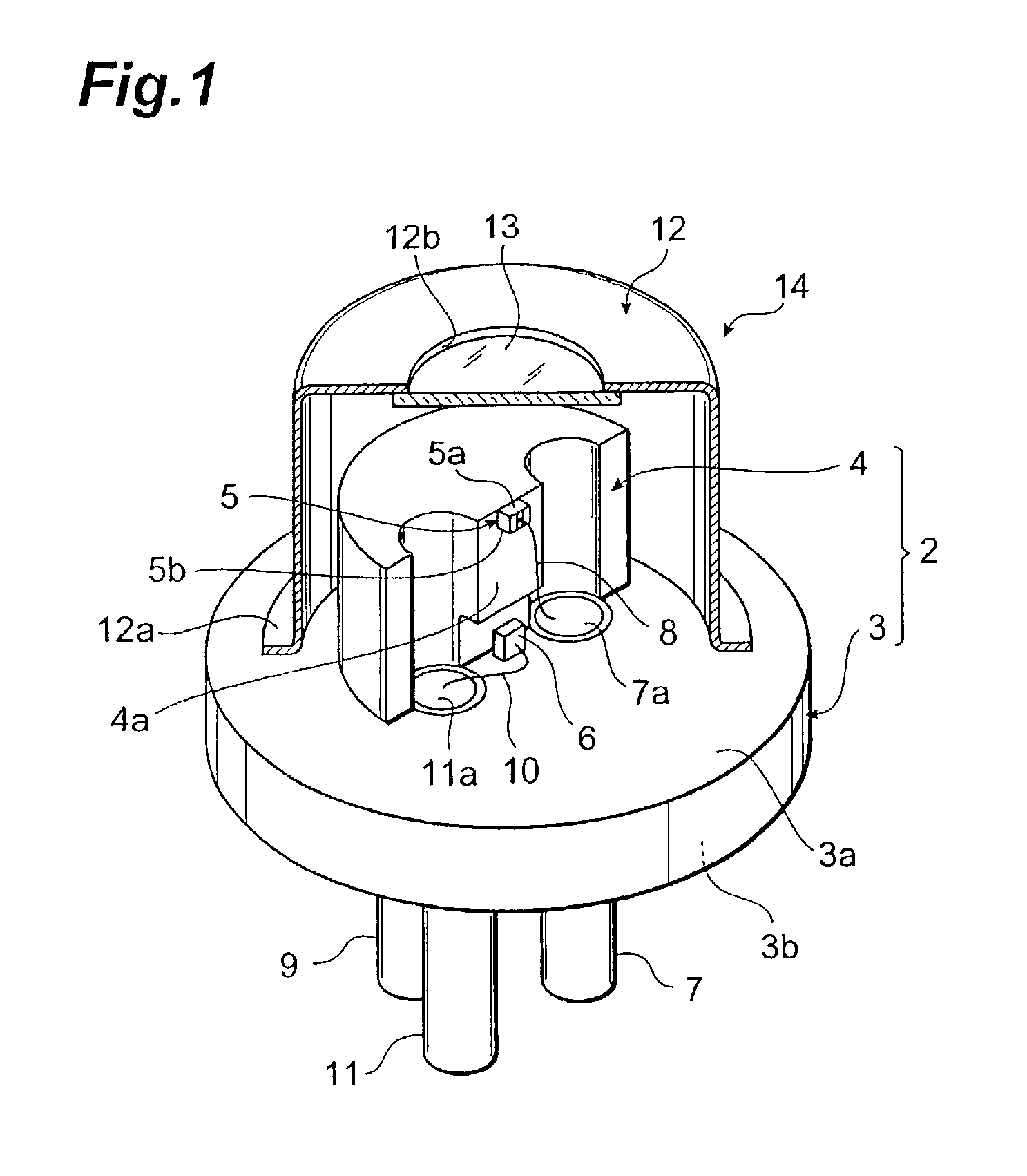
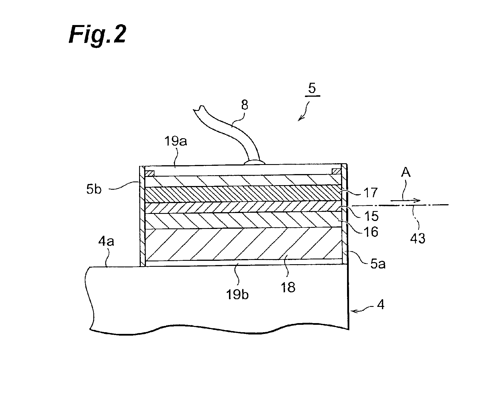
An embodiment of the present invention is described in detail below. FIG. 1 is a partly cutaway perspective view illustrating an embodiment of an excitation light source device used in an optical amplifier according to the present invention, being a so-called non-temperature regulated excitation light source device. As shown in FIG. 1, excitation light source device 1 comprises a mounting member made of metal called a stem 2. This stem 2 comprises a disc-shaped base 3 and a mounting portion 4 which is half-moon shaped in cross section. Base 3 has a flat face 3a and a mounting portion 4 is provided so as to extend integrally from flat face 3a. Mounting portion 4 comprises a mounting face 4a which is perpendicular with flat face 3a; a semiconductor laser element 5 that generates laser light is fixed by solder or the like to mounting face 4a. Semiconductor laser element 5 comprises a first end face 5a that emits the laser beam and a second end face 5b opposite to first end face 5a, fir...


PUM


Abstract

Optical amplifier according to the present invention is provided with an EDF, a light source device having a semiconductor laser element that generates an excitation beam and a housing that accommodates this, and an optical multiplexer having an input optically coupled with light source device, an input that receives the signal beam, and an output that provides an excitation beam and signal beam to EDF. Semiconductor laser element has an active layer, provided between cladding layers and including compound semiconductors of mutually different conductivity types, that includes a compound semiconductor and is constructed such that the oscillation wavelength at 20° C. of this semiconductor laser element is less than 1470 nm but not less 1440 nm. If this is done, the change of gain in EDF with respect to oscillation wavelength can be made satisfactorily small and the NF can be made satisfactorily small.

Description

BACKGROUND OF THE INVENTION1. Field of the InventionThe present invention relates to an optical amplifier.2. Related Background ArtIn WDM (Wavelength Division Multiplexing) transmission systems, in which signal beams consisting of components of a large number of wavelengths are transmitted by introducing these simultaneously into an optical fiber path, optical amplifiers are employed at relay stations etc to make up for transmission losses occurring when these signal beams of multiple wavelengths are transmitted over a long distance. In addition, optical amplifiers are likewise employed to make up transmission losses in passive optical devices (such as for example AWG: Arrayed Wavelength Grating) within relay stations.Such optical amplifiers are constituted comprising an optical amplification section that amplifies an input signal beam before outputting it and that is obtained by doping with a fluorescent substance capable of excitation by an excitation beam, and an excitation light...

Claims


Application Information

Patent Timeline
Patent Type & Authority Patents(United States)
IPC IPC(8): H01S5/00H01S5/022H01S5/343H01S3/06H01S3/16H01S3/094H01S3/067H01S5/028
CPCB82Y20/00H01S5/02212H01S3/06754H01S3/094003H01S5/3434H01S5/028H01S3/1608
Inventor NAKAZAWA, SATORUMURAKAMI, YASUNORI
Owner SUMITOMO ELECTRIC IND LTD
Learn More