Device and method for protecting against oxidation of a conductive layer in said device

Inactive Publication Date: 2005-02-08
APTINA IMAGING CORP
View PDF63 Cites 0 Cited by
  • Summary
  • Abstract
  • Description
  • Claims
  • Application Information

AI Technical Summary

Benefits of technology

Accordingly, the current invention provides a method for protecting a conductive layer from oxygen. At least one exemplary embodiment concerns preventing or at least limiting a first conductive layer from incorporating oxygen beneath the layer's surface. Other exemplary embodiments address methods of limiting the first conductive layer's ability to adsorb oxygen. In doing so, such embodiments can help prevent the diffusion of oxygen into a second conductive layer, thereby protecting against oxidation between conductive layers. One such method serving as an exemplary embodiment involves exposing one of the conductive layers to an N2 / H2 plasma before another conductive layer is provided thereon. In a preferred embodiment, this step is performed in situ relative to the environment or ambient atmosphere in which the one conductive layer was provided.

Problems solved by technology

If polysilicon is deposited directly onto tantalum pentoxide, however, several problems will occur.
First, silicon may diffuse into the tantalum pentoxide, thus degrading it.
Second, oxygen will migrate from the tantalum pentoxide, resulting in a capacitor that leaks charge too easily.
Further, the oxygen migrates to the polysilicon, creating a layer of non-conductive oxide, which decreases the capacitance.
This can also be a problem when using barium strontium titanate ((Ba, Sr)TiO3, or BST) as the dielectric.
However, other problems arise with this process.
Other problems can occur with the association of WNx and Ta2O5.
If the interface is exposed to an ambient containing oxygen, then a thermal process involving the alloying or flowing of the metal in the metal line could cause a similar problem with oxidation, thereby hindering electrical contact.

Method used


Image

  • Device and method for protecting against oxidation of a conductive layer in said device
  • Device and method for protecting against oxidation of a conductive layer in said device
  • Device and method for protecting against oxidation of a conductive layer in said device

Examples


Embodiment Construction

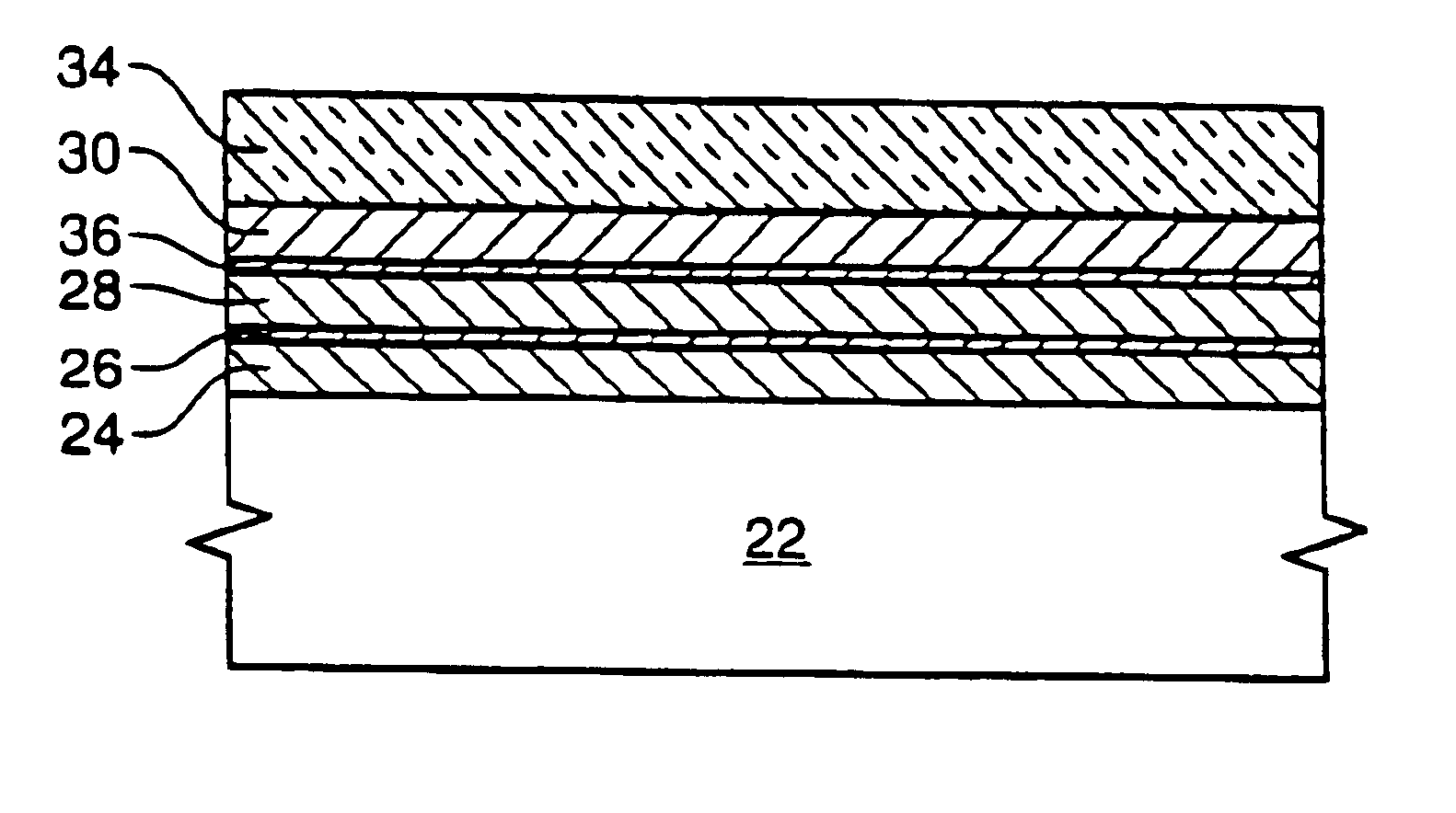
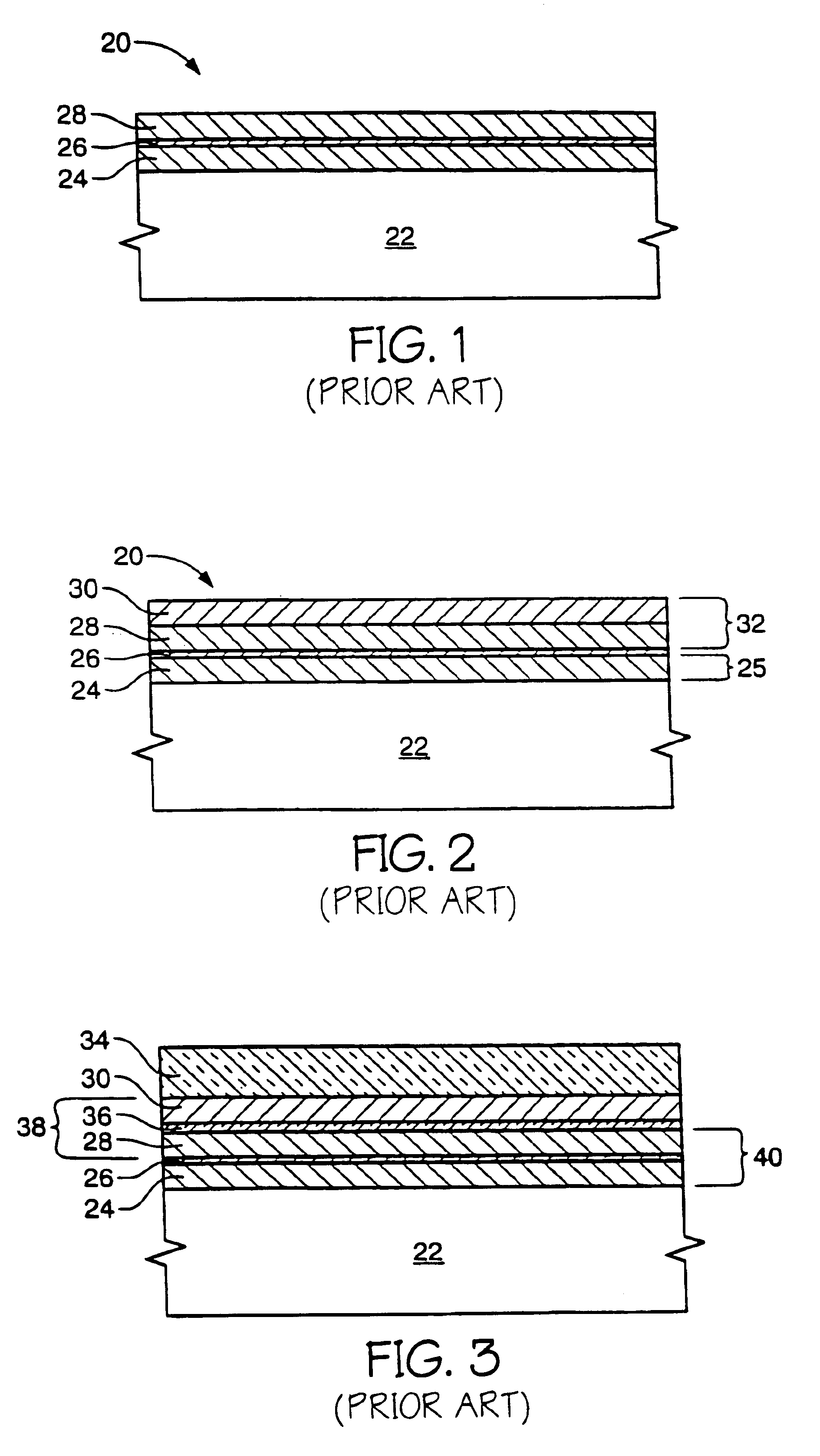
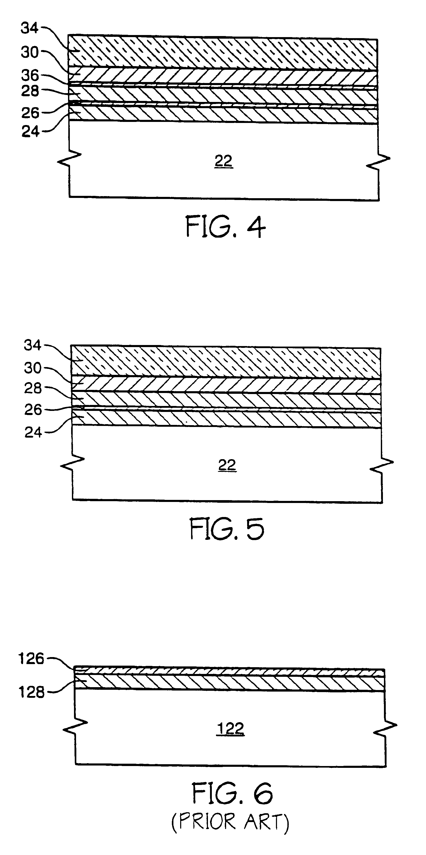
FIG. 1 depicts an “in-process” device 20—one that is in the process of being constructed—having undergone processes known in the art. First, a substrate 22 has been provided. In the current application, the term “substrate” or “semiconductor substrate” will be understood to mean any construction comprising semiconductor material, including but not limited to bulk semiconductive materials such as a semiconductor wafer (either alone or in assemblies comprising other materials thereon), and semiconductive material layers (either alone or in assemblies comprising other materials). Further, the term “substrate” also refers to any supporting structure including, but not limited to, the semiconductive substrates described above. Over the substrate 22, a first conductive layer 24 is provided. It is assumed for purposes of explanation only that the in-process device is a capacitor in the process of being built. Accordingly, the first conductive layer 24 serves as one of the capacitor's condu...


PUM


Abstract

In a semiconductor device including a first conductive layer, the first conductive layer is treated with a nitrogen / hydrogen plasma before an additional layer is deposited thereover. The treatment stuffs the surface with nitrogen, thereby preventing oxygen from being adsorbed onto the surface of the first conductive layer. In one embodiment, a second conductive layer is deposited onto the first conductive layer, and the plasma treatment lessens if not eliminates an oxide formed between the two layers as a result of subsequent thermal treatments. In another embodiment, a dielectric layer is deposited onto the first conductive layer, and the plasma treatment lessens if not eliminates the ability of the first conductive layer to incorporate oxygen from the dielectric.

Description

TECHNICAL FIELDThe present invention relates generally to a method of protecting against a conductive layer incorporating oxygen and a device including that layer. More specifically, the present invention relates to an in situ treatment of tungsten nitride.BACKGROUND OF THE INVENTIONThere is a constant need in the semiconductor industry to increase the number of dies that can be produced per silicon wafer. This need, in turn, encourages the formation of smaller die. Accordingly, it would be beneficial to be able to form smaller structures and devices on each die without losing performance. For example, as capacitors are designed to take an ever decreasing amount of die space, those skilled in the relevant art have sought new materials with which to maintain or even increase capacitance despite the smaller size.One such material is tantalum pentoxide (Ta2O5), which can be used as the dielectric in the capacitor. Oftentimes, an electrically conductive layer, such as one made of hemisp...

Claims


Application Information

Patent Timeline
IPC IPC(8): H01L21/02H01L21/70H01L21/8242
CPCH01L28/40H01L28/75H01L27/1085Y10S438/957Y10S438/958H10B12/03
Inventor AGARWAL, VISHNU K.
Owner APTINA IMAGING CORP
Why Eureka
Try Eureka