
Defect detection and repair of micro-electro-mechanical systems (MEMS) devices

a technology of micro-electro-mechanical systems and defects, applied in individual semiconductor device testing, semiconductor/solid-state device testing/measurement, instruments, etc., can solve problems such as adverse effects on the performance of mems devices, and achieve the effect of efficient detection and repair of mechanical as well as electrical defects

Inactive Publication Date: 2005-01-25
II VI DELAWARE INC
View PDF1 Cites 113 Cited by
  • Summary
  • Abstract
  • Description
  • Claims
  • Application Information

AI Technical Summary

Benefits of technology

To address the shortcomings of the available art, the present invention provides for a metho

Problems solved by technology

In general, performance of MEMS devices is adversely affected by the presence of various defects, including mechanical defects as well as electrical defects.
Indeed, a typical movable actuator or sensor formed by micromachining the substrate is highly sensitive to the presence of different defects on its surface, as well in its volume, including mechanical and ‘short’ and / or ‘open’ electrical defects.

Method used


Image

  • Defect detection and repair of micro-electro-mechanical systems (MEMS) devices
  • Defect detection and repair of micro-electro-mechanical systems (MEMS) devices
  • Defect detection and repair of micro-electro-mechanical systems (MEMS) devices

Examples


example i

Biotechnology

MEMS technology is enabling new discoveries in science and engineering such as the Polymerase Chain Reaction (PCR) microsystems for DNA amplification and identification, micromachined Scanning Tunneling Microscopes (STMs), biochips for detection of hazardous chemical and biological agents, and microsystems for high-throughput drug screening, delivery and selection.

example ii

Communications

High frequency circuits will benefit considerably from the advent of the Radio Frequency (RF)-MEMS technology. Electrical components such as tunable inductors, and tunable capacitors, filters, etc. can be improved significantly compared to their integrated bulk counterparts if they are made using MEMS technology. With the integration of such components, the performance of communication circuits will improve, while the total circuit area, power consumption and cost will be reduced. In addition, the mechanical switch, as developed by several research groups, is a key component with huge potential in various microwave circuits. The demonstrated samples of mechanical switches have quality factors much higher than anything previously available. Reliability and packaging of RF-MEMS components seem to be the two critical issues that need to be solved before they receive wider acceptance by the market.

example iii

Accelerometers

MEMS accelerometers are quickly replacing conventional accelerometers for crash air-bag deployment systems in automobiles. The conventional approach uses several bulky accelerometers made of discrete components mounted in the front of the car with separate electronics near the air-bag; this approach costs over $50 per automobile. MEMS technology has made it possible to integrate the accelerometer and electronics onto a single silicon chip at a cost between $5 to $10. These MEMS accelerometers are much smaller, more functional, lighter, more reliable, and are produced for a fraction of the cost of the conventional macroscale accelerometer elements.


PUM


Abstract

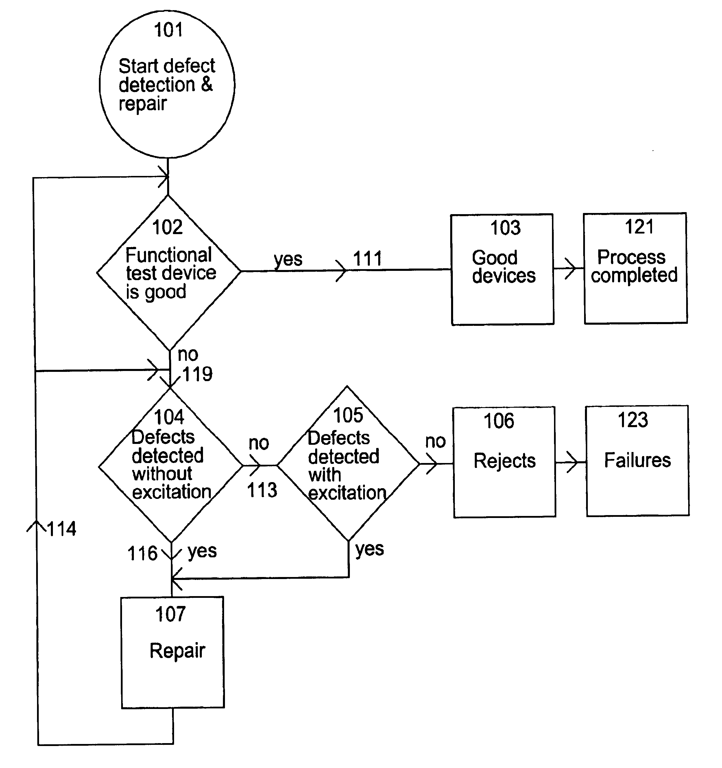
A method of defect detection and repair of micro-electro-mechanical systems (MEMS) devices comprising the steps of (A) detecting at least one defect in the MEMS device, wherein each defect is an object that prevents the MEMS device from functioning substantially properly; (B) performing repair of each detected defect; (C) checking whether the MEMS device is functioning substantially properly after each detected defect is repaired; and (D) if the MEMS device is not functioning substantially properly after each detected defect is repaired, repeating steps (A-C).

Description

BACKGROUND OF THE INVENTION1. Field of the InventionThe present invention relates to the field of micro-electro-mechanical systems (MEMS) devices, and more specifically, to the field of detection and repair of defects that substantially prevent MEMS devices from functioning properly.2. Discussion of the Prior ArtMicro engineered devices such as micro-electro-mechanical structures (MEMS) are presently being developed for a wide variety of applications in view of the size, cost and reliability advantages provided by these devices. For example, one advantageous MEMS device is a variable capacitor in which the interelectrode spacing between a pair of electrodes is controllably varied in order to selectively vary the capacitance between the electrodes. Typically, a conventional MEMS variable capacitor includes a pair of electrodes, one of which is disposed upon and fixed to the substrate and the other of which is typically carried on a movable actuator or driver. In accordance with MEMS ...

Claims


Application Information

Patent Timeline
IPC IPC(8): G01R31/26G06F19/00B81C99/00G01Q30/02G01Q60/00G01Q80/00G01Q90/00
CPCB81C99/0045Y10S977/855
Inventor NOVOTNY, VLAD J.
Owner II VI DELAWARE INC
Learn More