Non-volatile semiconductor memory with single layer gate structure

a non-volatile, gate-based technology, applied in the direction of semiconductors, electrical devices, transistors, etc., can solve the problems of increasing the number of fabrication steps and fabrication costs, increasing the accuracy requirements of the element, and the structure of the non-volatile semiconductor memory is complicated, so as to achieve reliable semiconductors, reduce the variation of threshold values, and perform write and read operations stably

Inactive Publication Date: 2005-01-04
INTELLECTUAL VENTURES I LLC
View PDF11 Cites 11 Cited by
  • Summary
  • Abstract
  • Description
  • Claims
  • Application Information

AI Technical Summary

Benefits of technology

It is an object of the present invention to provide a reliable semiconductor device which is a single-layer gate semiconductor device by which a low-cost process is possible, has a control gate which can well withstand a high voltage applied when data is erased or written, and can prevent an operation error, and a method of fabricating the same.
In the present invention, a conductor layer which functions as the control gate of a nonvolatile semiconductor memory is formed in a surface region of a semiconductor substrate, and a region from the side surfaces to the lower surface of this conductor layer is completely covered with an insulating film. Therefore, even when a high voltage is applied to the control gate to erase data, a high breakdown voltage can be held in the outer portion of the conductor layer. Also, a pair of diffusion layers is formed in surface regions of the semiconductor substrate on the two sides of a tunnel oxide film of the nonvolatile semiconductor memory, and an electrode is formed to apply a predetermined substrate potential to an element active region including these diffusion layers. Accordingly, it is possible to minimize variation in the threshold value and stably perform write and read operations.
The present invention can realize a reliable semiconductor device which is a single-layer gate semiconductor device by which a low-cost process is possible, has a control gate which can well withstand a high voltage applied when data is erased or written, and can prevent an operation error.

Problems solved by technology

However, the structure of this nonvolatile semiconductor memory is complicated because the memory has a stacked gate structure, and this extremely increases the accuracy requirements when the element is to be formed.
This not only increases the number of fabrication steps and the fabrication cost and lowers the reliability but also interferes with an increase in the degree of integration.
Consequently, it becomes difficult to ensure a large enough breakdown voltage between the control gate and the semiconductor substrate, leading to a serious problem of an operation error.
However, it is difficult to minimize variations in the threshold value of the EEPROM and stably perform write and read operations.

Method used


Image

  • Non-volatile semiconductor memory with single layer gate structure
  • Non-volatile semiconductor memory with single layer gate structure
  • Non-volatile semiconductor memory with single layer gate structure

Examples


first embodiment -

-First Embodiment-

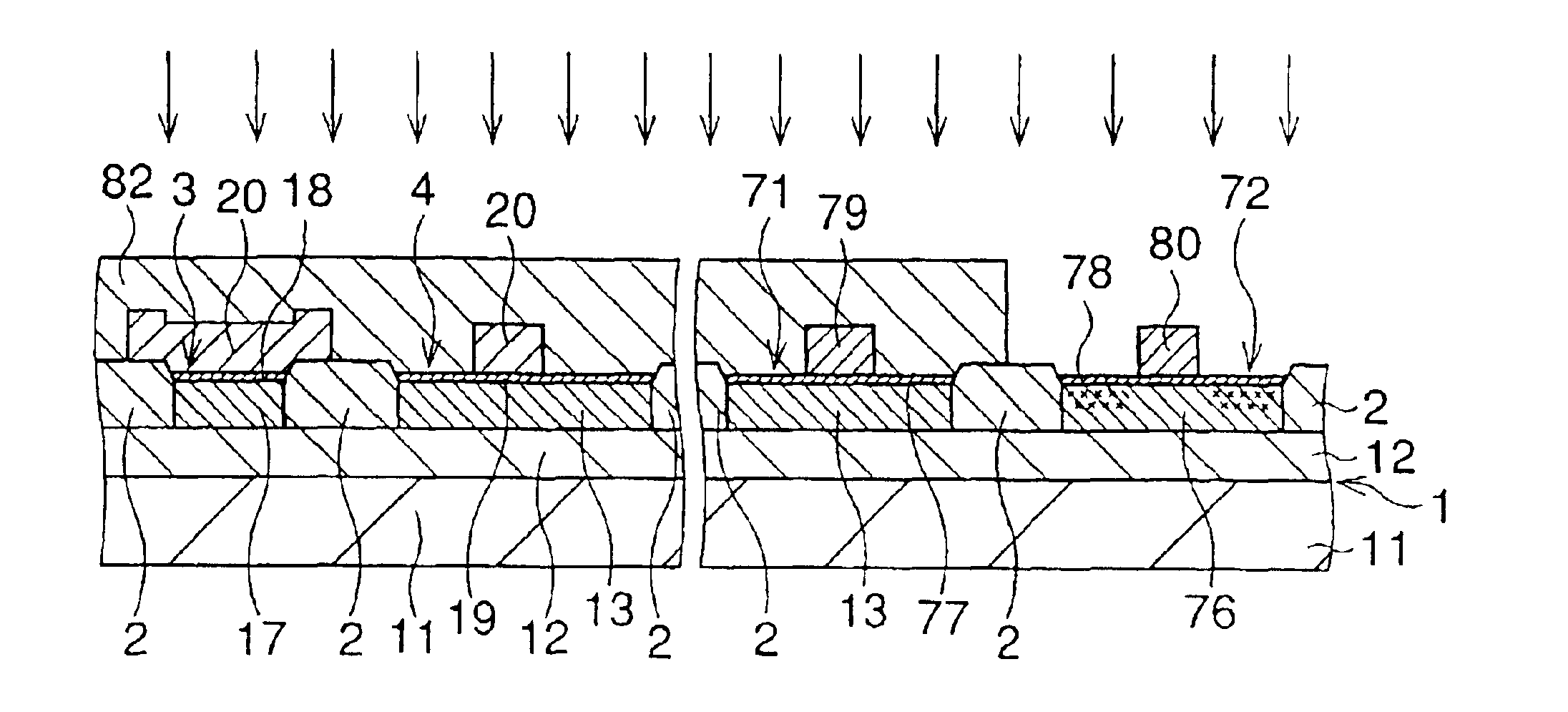
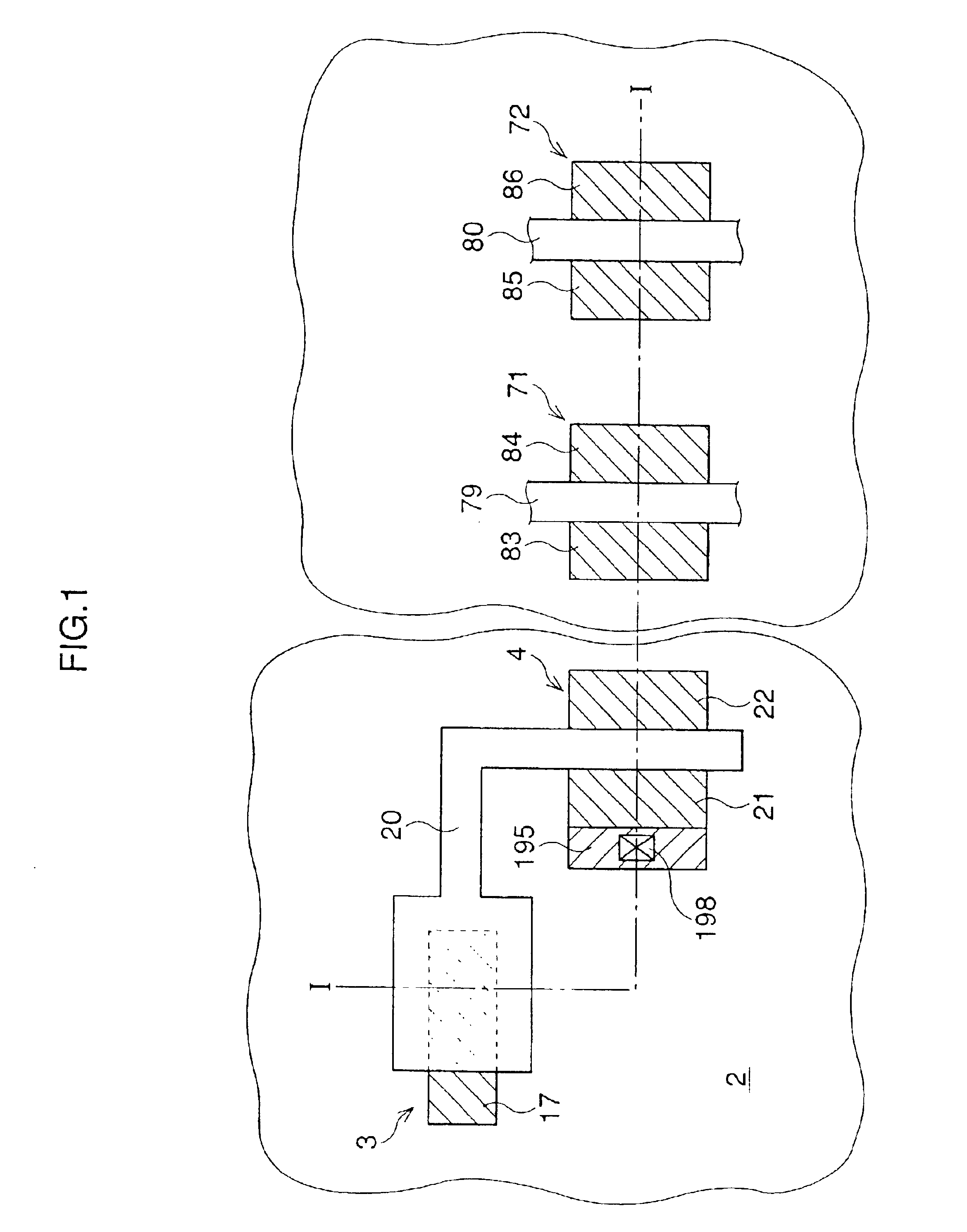
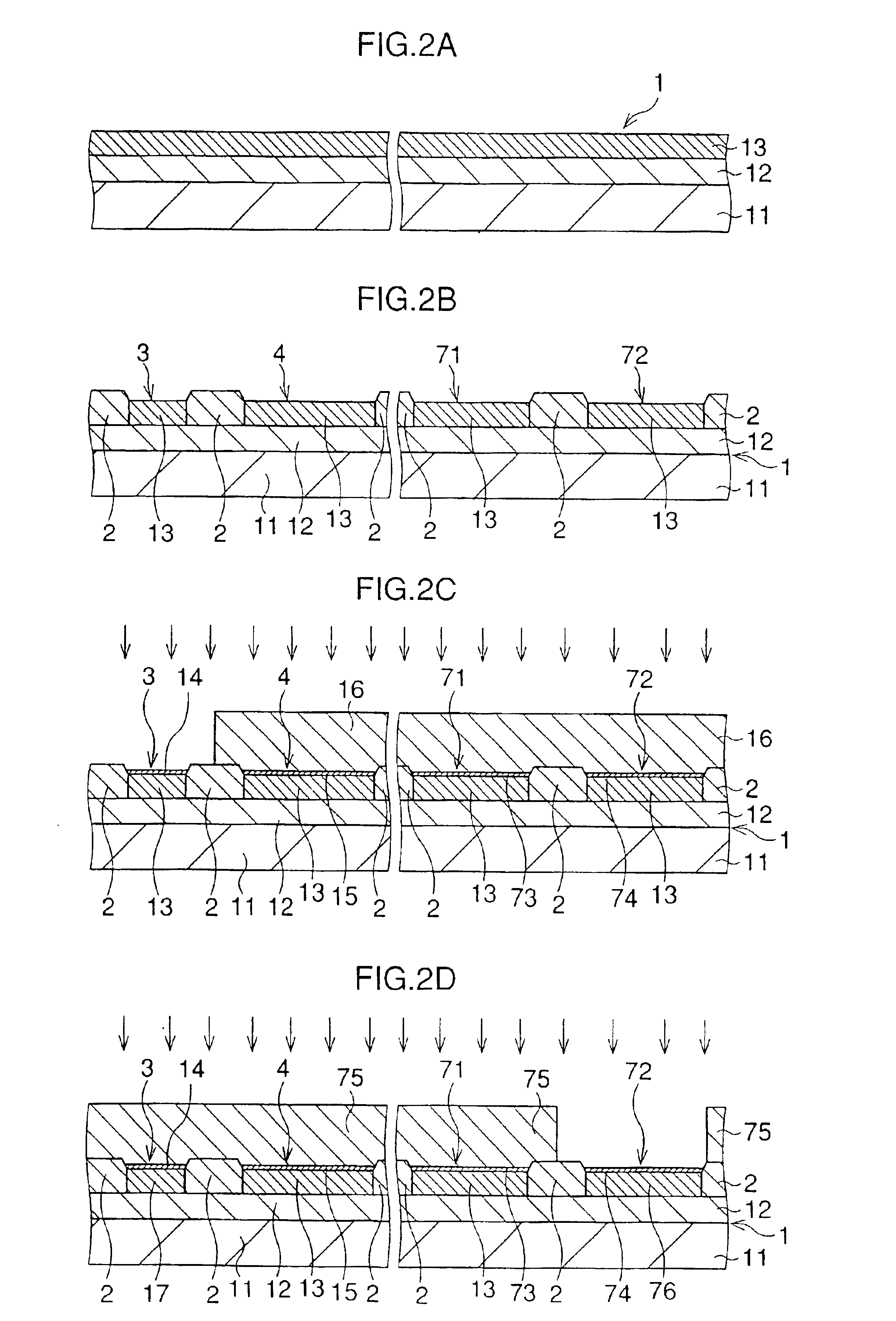
The first embodiment will be described below. In this first embodiment, an EEPROM as a nonvolatile semiconductor memory will be exemplified as a semiconductor device, and the structure and the fabrication method of this EEPROM will be explained. Also, a method of forming a CMOS inverter as a peripheral circuit simultaneously with the formation of the EEPROM will be explained. FIG. 1 is a schematic plan view showing the EEPROM and the CMOS inverter. FIGS. 2A to 2I are schematic sectional views, taken along an alternate long and short dashed line I—I in FIG. 1, showing the fabrication method of the EEPROM and the CMOS inverter in order of steps.

First, as shown in FIG. 2A, an SOI substrate 1 is prepared by forming a single-crystal silicon layer 13 about 50 nm thick on a p-type silicon semiconductor substrate 11 via a buried oxide film 12 about 50 nm thick.

Next, as shown in FIG. 2B, the SOI substrate 1 is selectively oxidized to form a field oxide film 2 about 100 nm t...

second embodiment -

-Second Embodiment-

The second embodiment of the present invention will be described below. In this second embodiment, the structure and the fabrication method of an EEPROM will be explained as in the first embodiment. However, the second embodiment differs from the first embodiment in that no SOI substrate is used and trench isolation is used as element isolation. FIG. 4 is a schematic plan view showing this EEPROM. FIGS. 5A to 5I are schematic sectional views, taken along an alternate long and short dashed line I—I in FIG. 4, showing the method of fabricating the EEPROM in order of steps performed. Note that the same reference numerals as in the EEPROM of the first embodiment denote the same parts in the second embodiment and a detailed description thereof will be omitted.

First, as shown in FIG. 5A, the surface of a p-type silicon semiconductor substrate 31 is coated with a photoresist about 1.5 μm thick via a silicon oxide film 32 about 50 nm thick. This photoresist is processed b...

third embodiment -

-Third Embodiment-

The third embodiment of the present invention will be described below. In this third embodiment, the structure and the fabrication method of an EEPROM will be explained as in the first embodiment. However, the third embodiment differs from the first embodiment in that a SIMOX method is used. FIG. 7 is a schematic plan view showing this EEPROM. FIGS. 8A to 8H are schematic sectional views, taken along an alternate long and short dashed line I—I in FIG. 7, showing the fabrication method of the EEPROM in order of steps. Note that the same reference numerals as in the EEPROM of the first embodiment denote the same parts in the third embodiment, and a detailed description thereof will be omitted.

First, as shown in FIG. 8A, a silicon oxide film 43 about 1.5 to 2.0 μm thick is deposited by CVD on a p-type single-crystal silicon semiconductor substrate 41 via a silicon oxide film 42 about 100 nm thick. Photolithography and dry etching are sequentially performed on this sil...


PUM


Abstract

A semiconductor device of this invention is a single-layer gate nonvolatile semiconductor memory in which a floating gate having a predetermined shape is formed on a semiconductor substrate. This floating gate opposes a diffusion layer serving as a control gate via a gate oxide film and is capacitively coupled with the diffusion layer by using the gate oxide film as a dielectric film. The diffusion layer immediately below the dielectric film is insulated from the semiconductor substrate by an insulating film such as a silicon oxide film. A pair of diffusion layers are formed in surface regions of the semiconductor substrate on the two sides of the floating gate extending on a tunnel oxide film. This invention can realize a reliable semiconductor device which is a single-layer gate semiconductor device by which a low-cost process is possible, has a control gate which can well withstand a high voltage applied when data is erased or written, and can prevent an operation error by minimizing variations in the threshold value.

Description

BACKGROUND OF THE INVENTION1. Field of the InventionThe present invention relates to a semiconductor device and to a method of fabricating the same. More particularly, it relates to semiconductor device suitably applicable to a nonvolatile semiconductor memory in which a floating gate and a control gate are formed via a dielectric film.2. Description of the Related ArtRecently, a nonvolatile memory such as an EEPROM which holds stored data even when disconnected from a power supply has attracted attention as a semiconductor memory. In this nonvolatile memory, a floating gate is formed on a semiconductor substrate via a tunnel insulating film, and a control gate is formed as to oppose this floating gate via a dielectric film.One example of this nonvolatile semiconductor memory is disclosed in Japanese Patent Laid-Open No. 6-85279. This element is obtained by turning the above nonvolatile semiconductor memory upside down. More specifically, this nonvolatile semiconductor memory is fab...

Claims


Application Information

Patent Timeline
Patent Type & Authority Patents(United States)
IPC IPC(8): H01L27/115H01L29/66H01L29/788H01L27/12H01L27/105H01L21/8247H01L21/76H01L29/792H10B20/00H10B69/00
CPCH01L29/7883H01L27/11502H01L27/105H01L27/1203H10B53/00
Inventor KUMAZAKI, YOSHIHIRO
Owner INTELLECTUAL VENTURES I LLC
Why Eureka
Try Eureka