
Laminate circuit structure and method of fabricating

a technology of laminate circuit and fabrication method, which is applied in the direction of conductive pattern formation, other domestic articles, and the improvement of the adhesion of the metal to the insulating substrate, etc., can solve the problems of exacerbate many of the problems associated with additional thickness, and achieve the effect of reducing costs

Inactive Publication Date: 2004-11-23
INT BUSINESS MASCH CORP
View PDF13 Cites 19 Cited by
  • Summary
  • Abstract
  • Description
  • Claims
  • Application Information

AI Technical Summary

Benefits of technology

This approach reduces thickness, improves adhesion, and enhances the reliability and cost-effectiveness of multilayer printed circuit boards by allowing direct adhesion of 2S1P cores and other layers without additional adhesive sheets, improving resistance to thermal cycling and electrical opens.

Problems solved by technology

These additional "sticker" sheets contribute additional thickness and exacerbate many of the problems associated with additional thickness.

Method used


Image

  • Laminate circuit structure and method of fabricating
  • Laminate circuit structure and method of fabricating
  • Laminate circuit structure and method of fabricating

Examples


Embodiment Construction

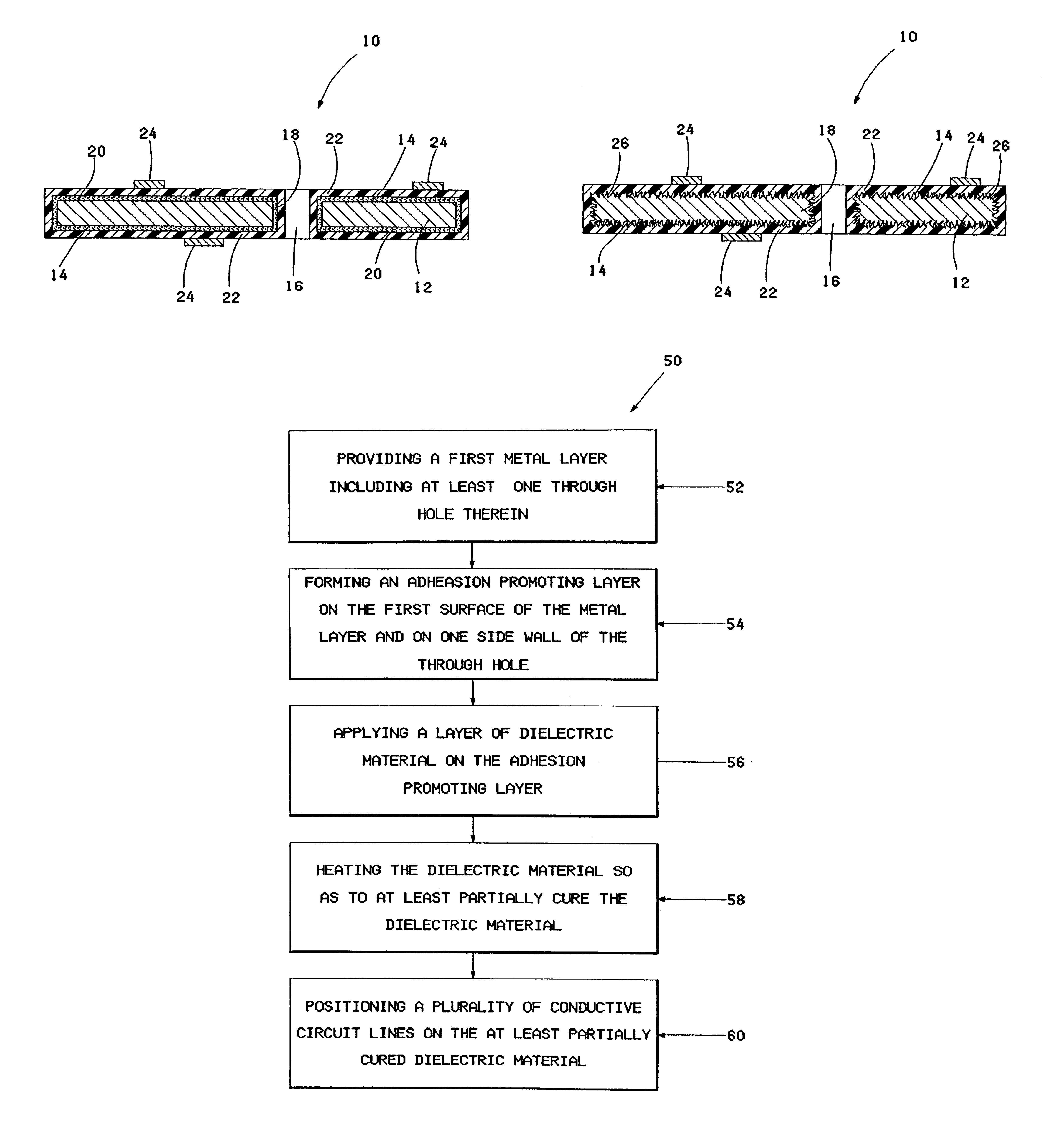
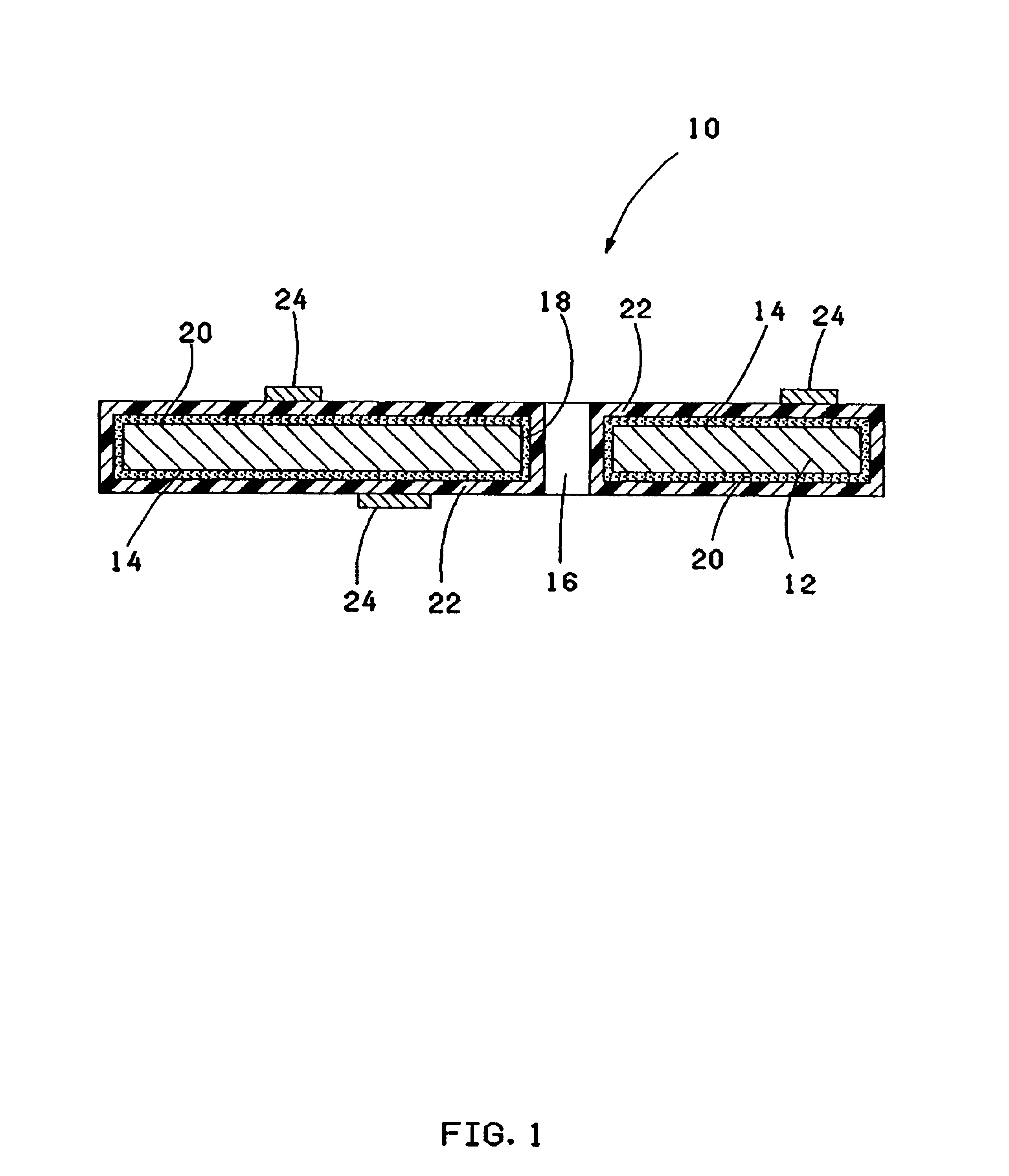
13 inch wide roll of 12.5% / 75% / 12.5% by weight copper / Invar / copper was coated on both sides with 12 mil. thick Dupont MI (1.5 mil. thick photo resist). The resist is exposed to 60 Millijoules of UV light on each side (one side is pattern imaged and the other side is blanket exposed) using a conventional PCB exposure machine. The roll is indexed through the exposure machine with one unit circuit board image exposed at a time. The completely exposed roll is then set up on a roll to roll Mylar peel / develop / etch / strip line and conventional chemical developing, etching and stripping is performed. Next the roll is moved to a roll to roll horizontal process tool capable of applying the Atotech Bondfilm(.TM.) treatment process for further processing. The step of forming the adhesion promoting layer includes the step of applying a coupling agent, a second metal layer, or a metal oxide, as described above, on the first surface of the first metal layer and on the at least one side wall of the ...


PUM

PropertyMeasurementUnit
dielectric loss tangentaaaaaaaaaa
sizesaaaaaaaaaa
particle diameter distributionsaaaaaaaaaa

Abstract

A substrate and a method of making the substrate is provided. The substrate includes a layer of metal with at least one through hole therein, the layer of metal having an adhesion promoting layer thereon. A layer of a partially cured low-loss polymer or polymer precursor is positioned on the adhesion promoting layer and a plurality of conductive circuit lines are positioned on a portion of the partially cured dielectric layer. The substrate can be used as a building block in the fabrication of a multilayered printed circuit board.

Description

The present invention relates to laminate circuit board structures for use in making multilayer printed circuit boards, and in particular to organic circuit board structures for use in such boards.A conventional technique of forming a laminate circuit board structure includes forming layers of dielectric material and layers of electrically conducting material to provide multiple layers of circuits, dielectrics, and voltage planes.Conventional multilayer printed circuit boards are typically constructed from glass cloth prepreg and copper. Normally copper clad laminates are circuitized and then "laid up" in a sequential fashion with other circuitized cores and additional sticker prepreg (sticker sheets) to form composites. Once laminated, conventional composite boards are drilled and then plated to form multilayer printed circuit boards.Composites constructed using 2 signal planes and one power (plane (2S1P) building block cores, offer a number of advantages over conventional construc...

Claims


Application Information

Patent Timeline
Patent Type & Authority Patents(United States)
IPC IPC(8): H05K3/38H05K1/05
CPCH05K1/056H05K3/382H05K3/388H05K3/383H05K3/384H05K3/389Y10T29/49165H05K2201/0209H05K2201/0355H05K2203/0307Y10S428/901Y10T29/49126Y10T29/49155H05K3/445
Inventor JAPP, ROBERT M.MARKOVICH, VOYA R.PAPATHOMAS, KONSTANTINOS I.
Owner INT BUSINESS MASCH CORP
Learn More