Dielectric ceramic composition and electronic device
a technology of ceramic composition and electronic device, which is applied in the direction of fixed capacitor details, inorganic insulators, fixed capacitors, etc., can solve the problems of increasing environmental stress on electronic devices, reducing specific resistance of dielectric layers, and insufficient material for electronic devices
- Summary
- Abstract
- Description
- Claims
- Application Information
AI Technical Summary
Benefits of technology
Problems solved by technology
Method used
Image
Examples
examples 10
d Comparative Examples 5.about.7
Prism-shaped ceramic sintered body samples and multi-layer ceramic capacitor samples were prepared in the same way as in Examples 1 to 9 excepting that Yb was added as a fourth subcomponent (an oxide of R1) by a composition amount to be 4.3 mol, Eu, Gd, Tb, Dy, Ho, Nb, Ta or Sm was added as a fifth subcomponent (an oxide of R2) respectively by a composition amount to be 2 mol as an element, and other additives were mixed by the amount shown in Table 2.
Characteristics of the samples are shown in Table 2 as the results of measuring in the same way as in the Examples 1 to 9.
TABLE 3
Evaluation
As shown in FIG. 2, it was confirmed that transverse strength is improved in the cases of the Examples 10 to 14 wherein Ho, Y, Dy, Eu, Gd or Tb was added comparing with the Comparative Example 1 in Table 1 wherein the fifth subcomponent (an oxide of R2) is not added. Also, it was confirmed that transverse strength is improved in the cases of the Examples 10 to 14 wher...
example 16
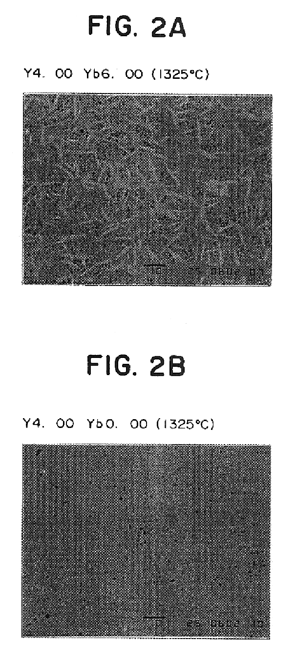
A prism-shaped ceramic sintered body sample was prepared in the same way as in the Example 1 excepting that Yb in the fourth subcomponent (an oxide of R1) was 6.00 mole %, Y in the fifth subcomponent (an oxide of R2) was 4.00 mole % and the sintering temperature was 1325.degree. C.
A SEM picture of the sample is shown in FIG. 2A. The SEM picture was taken by a scanning electronic microscope (SEM: production No. JSM-T300 manufactured by JEOL Ltd.), and conditions at the time of taking the picture was an accelerating voltage of 25 kV and a reflection electronic image was captured. The picture was taken with the magnifying power of 5000.
As shown in FIG. 2A, a plate-shaped or acicula deposition phase existing together in the dielectric base phase of BaTiO.sub.3 as the main component was observed.
example 17
A prism-shaped ceramic sintered body sample was prepared in the same way as in the Example 1 excepting that Yb in the fourth subcomponent (an oxide of R1) was 4.3 mole %, Y in the fifth subcomponent (an oxide of R2) was 8.00 mole % and the sintering temperature was 1325.degree. C.
The SEM picture of the sample was taken in the same way as in the Example 16. The picture is shown in FIG. 3A.
As shown in FIG. 3A, a plate-shaped or acicula deposition phase existing together in the dielectric base phase of BaTiO.sub.3 as the main component was observed.
PUM
| Property | Measurement | Unit |
|---|---|---|
| temperature | aaaaa | aaaaa |
| temperature | aaaaa | aaaaa |
| Curie temperature | aaaaa | aaaaa |
Abstract
Description
Claims
Application Information
 - R&D
- Intellectual Property
- Life Sciences
- Materials
- Tech Scout
- Unparalleled Data Quality
- Higher Quality Content
- 60% Fewer Hallucinations
Browse by: Latest US Patents, China's latest patents, Technical Efficacy Thesaurus, Application Domain, Technology Topic, Popular Technical Reports.
© 2025 PatSnap. All rights reserved.Legal|Privacy policy|Modern Slavery Act Transparency Statement|Sitemap|About US| Contact US: help@patsnap.com


