Liquid crystal device and driving method therefor
a technology of liquid crystal devices and driving methods, which is applied in static indicating devices, instruments, non-linear optics, etc., can solve the problems of difficult control of the nucleation threshold, difficult to achieve the effect of electrical field treatment, and difficult to achieve the effect of reducing the number of pixel electrodes
- Summary
- Abstract
- Description
- Claims
- Application Information
AI Technical Summary
Problems solved by technology
Method used
Image
Examples
example 1
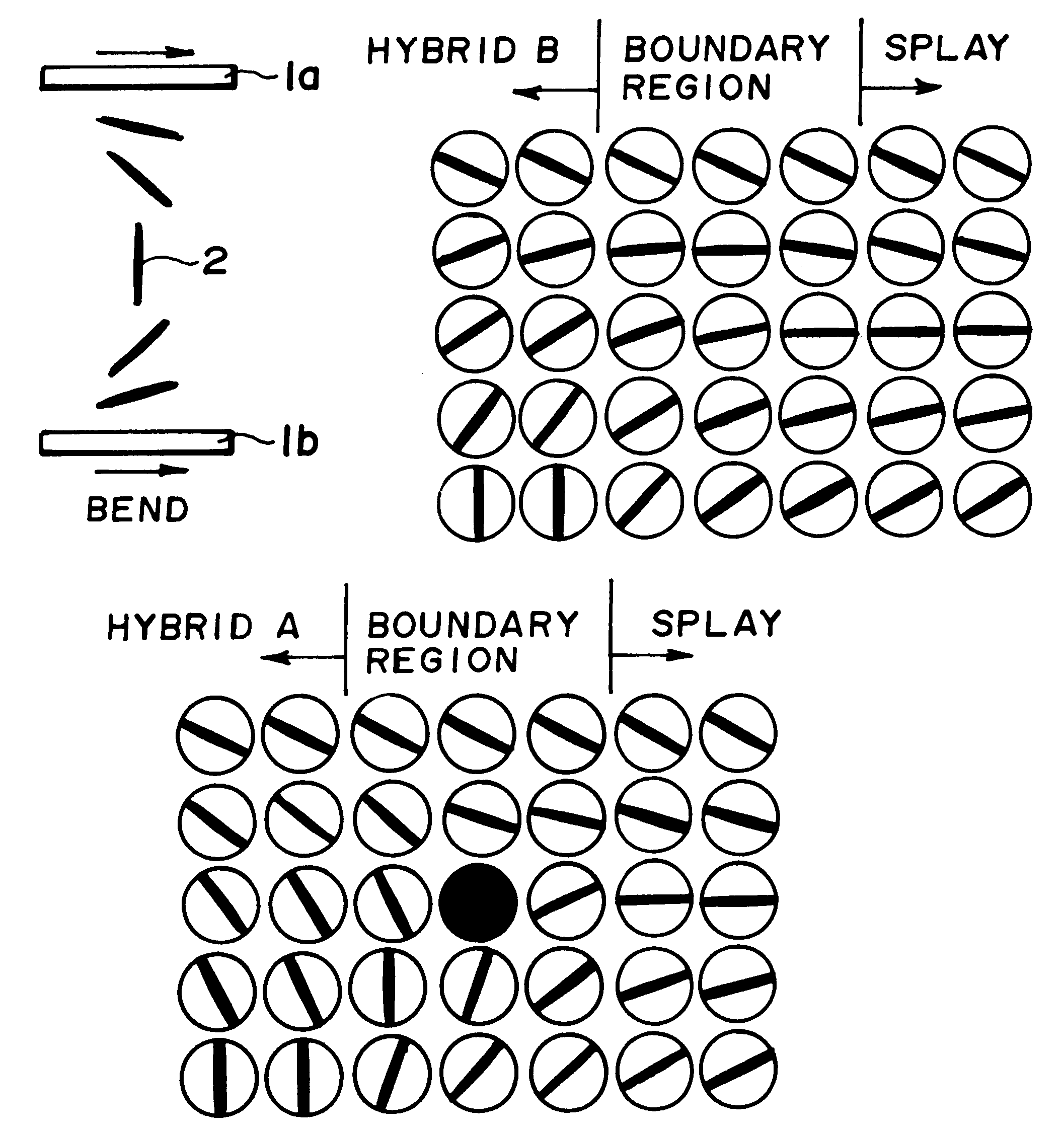
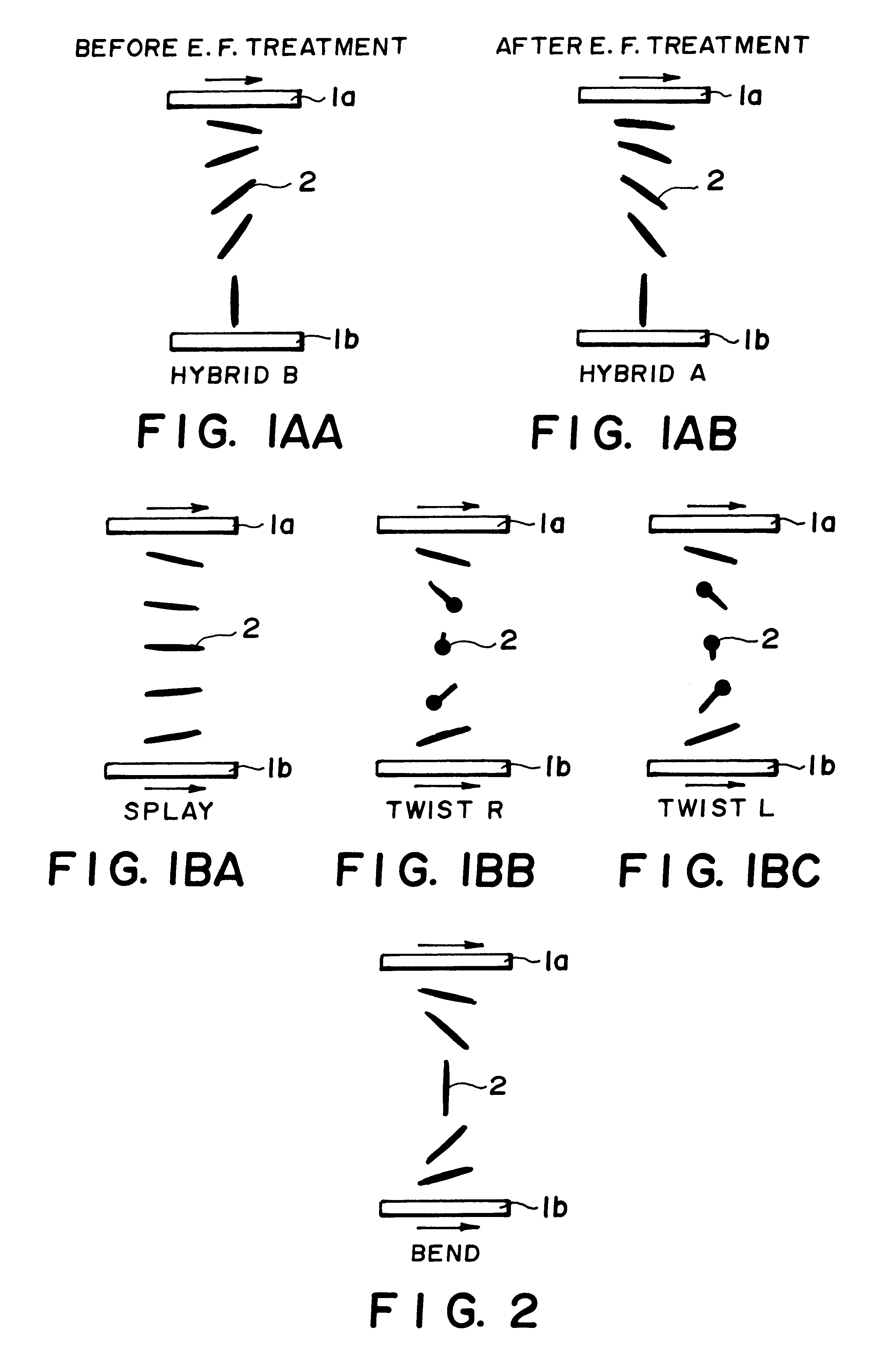
A liquid crystal device including a hybrid alignment region was prepared. The composite alignment film was prepared through a process as described with reference to FIGS. 14A-14D. Thus, referring to these figures, a glass substrate 32 was coated with a 150 nm-thick transparent electrode 33 of ITO of 1 cm.times.1 cm by vacuum deposition and then with 100 nm-thick insulating layer 34 of Ta.sub.2 O.sub.5. Thereon, an alignment film material ("LQ1800" available from Hitachi Kasei K.K.) was applied by spin coating, followed by baking at 270.degree. C. for 20 min. on a hot plate to form a 20 nm-thick alignment film 35a. Then, a photomask resist ("TPAR", available from Tokyo Ohka K.K.) was formed in a prescribed pattern 71, followed by rubbing and peeling of the resist 71. The rubbing intensity was adjusted to provide a pretilt angle of 10 deg. As a result, a first substrate having thereon a 1 cm.times.1 cm wide square electrode on which a homeotropic alignment film pattern 35a was formed ...
example 2
A liquid crystal device having a sectional structure as shown in FIG. 10 was prepared by using a TFT substrate instead of the second substrate in Example 1 and drive characteristics after optical compensation were examined. A hybrid alignment film region 35a was formed so as to cover spacings between pixel electrodes 30. Each TFT 27 was provided with a semiconductor layer 23 of ca. 200 nm-thick a-Si formed by glow discharge decomposition. The retention capacitance 29 was set to ca. 9 pF.
Drive voltages of .+-.2.0 volts and .+-.5.2 volts were used, and the bending treatment was performed by alternately applying a rectangular signal of 5.3 volts and 60 Hz and zero volt.
The liquid crystal device was driven by a set of drive signal voltage waveforms shown in FIG. 16 set to V.sub.+g =10 volts, V.sub.-g =-10 volts, .DELTA.T=16 .mu.sec, data signal voltages of .+-.2.0 volts to .+-.5.3 volts for picture display, and a common electrode potential set to a reference potential. A retardation dif...
example 3
A liquid crystal device having a structure identical to that of Example 2 was prepared except for changing the alignment film material and the liquid crystal material. The composite alignment film on the first substrate was prepared through a process as illustrated in FIGS. 15A-15D. More specifically, an ITO film 33 on a first substrate 32 was further coated with an insulating layer 34 of 100 nm-thick Ta.sub.2 O.sub.5 formed by vacuum deposition and then with an alignment film material ("AL-0656", available from Nippon Gosei Gomu K.K.) by spin coating, followed by baking at 200.degree. C. for 30 nm, to form a 50 nm-thick alignment film 41. Then, a photoresist ("OFPR 800" available from Tokyo Ohka K.K.) was formed in a pattern 71 for protecting a desired homogeneous alignment film region, and then contacted with a solution in a mixture solvent of water and IPA (isopropyl alcohol) of surface treating agent ("FC-805" available from 3M Co.) for providing a homeotropic alignment film reg...
PUM
 Abstract
Description
Claims
Application Information
 - R&D
- Intellectual Property
- Life Sciences
- Materials
- Tech Scout
- Unparalleled Data Quality
- Higher Quality Content
- 60% Fewer Hallucinations
Browse by: Latest US Patents, China's latest patents, Technical Efficacy Thesaurus, Application Domain, Technology Topic, Popular Technical Reports.
© 2025 PatSnap. All rights reserved.Legal|Privacy policy|Modern Slavery Act Transparency Statement|Sitemap|About US| Contact US: help@patsnap.com


