
Method of forming STI oxide regions and alignment marks in a semiconductor structure with one masking step

a technology of alignment marks and semiconductors, applied in semiconductor/solid-state device manufacturing, basic electric elements, electric devices, etc., can solve the problems of consuming expensive photoresist materials, kv masking steps that affect both cycle-time and tool capacity, and only create recesses for alignment marks, so as to improve process cycle-time and tool capacity, and reduce overall manufacturing costs

Inactive Publication Date: 2002-07-09
IBM CORP
View PDF6 Cites 20 Cited by
  • Summary
  • Abstract
  • Description
  • Claims
  • Application Information

AI Technical Summary

Benefits of technology

It is another object of the present invention to provide a method of forming the STI oxide regions and alignment marks in a semiconductor structure provided with deep trenches in DRAM / EDRAM chips which avoids the masking step usually referred to as the KV mask.
It is still another object of the present invention to provide a method of forming the STI oxide regions and alignment marks in a semiconductor structure provided with deep trenches in DRAM / EDRAM chips which improves process cycle-time and tool capacity to reduce the overall manufacturing costs.
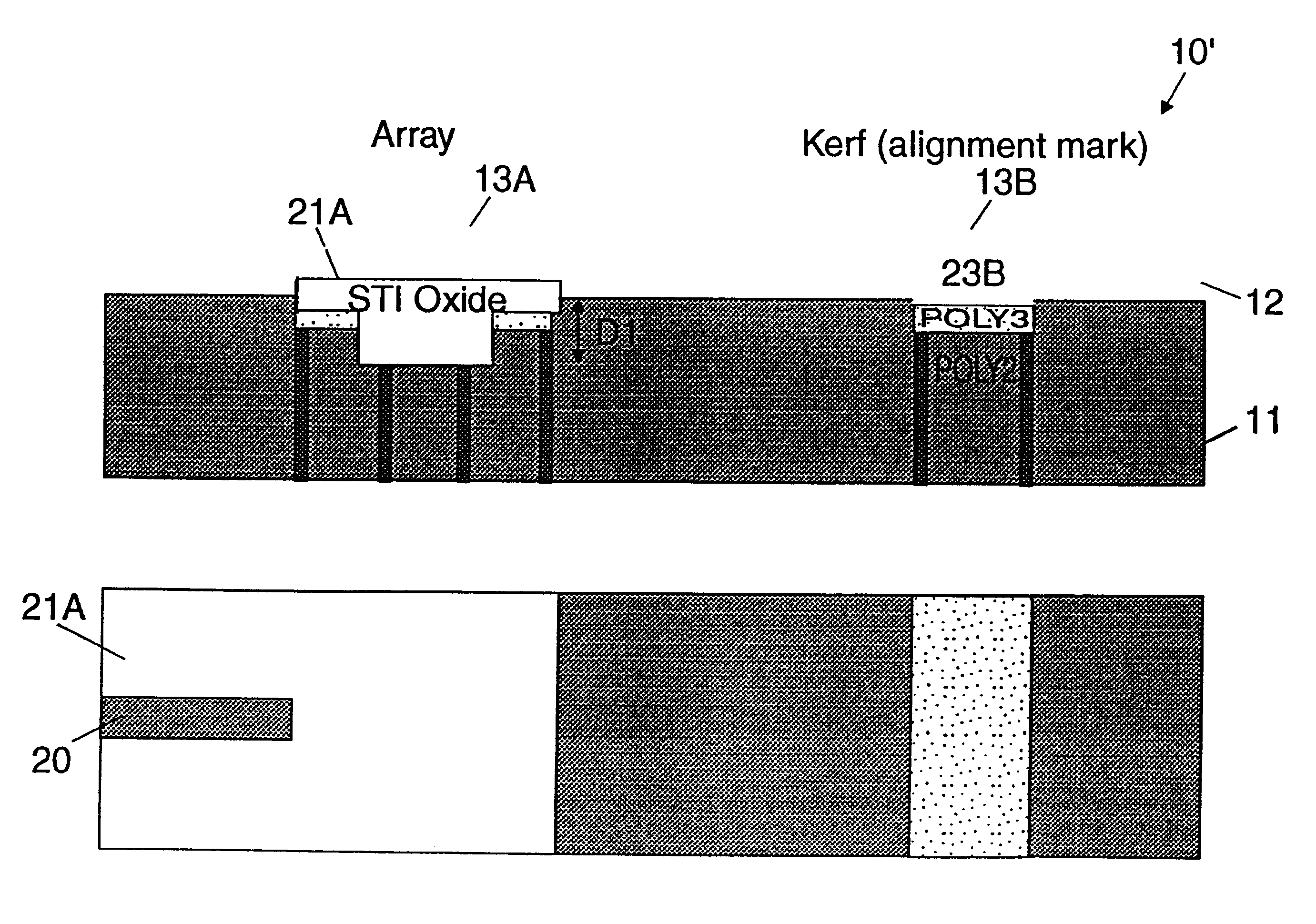
The method of the present invention thus allows the simultaneous formation of the STI oxide regions and the alignment marks. An important aspect of the method of the present invention is to leave polysilicon (POLY3) in the deep trenches to create recesses to be subsequently used as alignment marks in the "kerf" areas, preventing them from being filled by the STI oxide and then to create recesses without using any mask by etching selectively to the STI oxide. This process also allows the formation of polysilicon (POLY3) bumps if so desired to be subsequently used as alignment marks.

Problems solved by technology

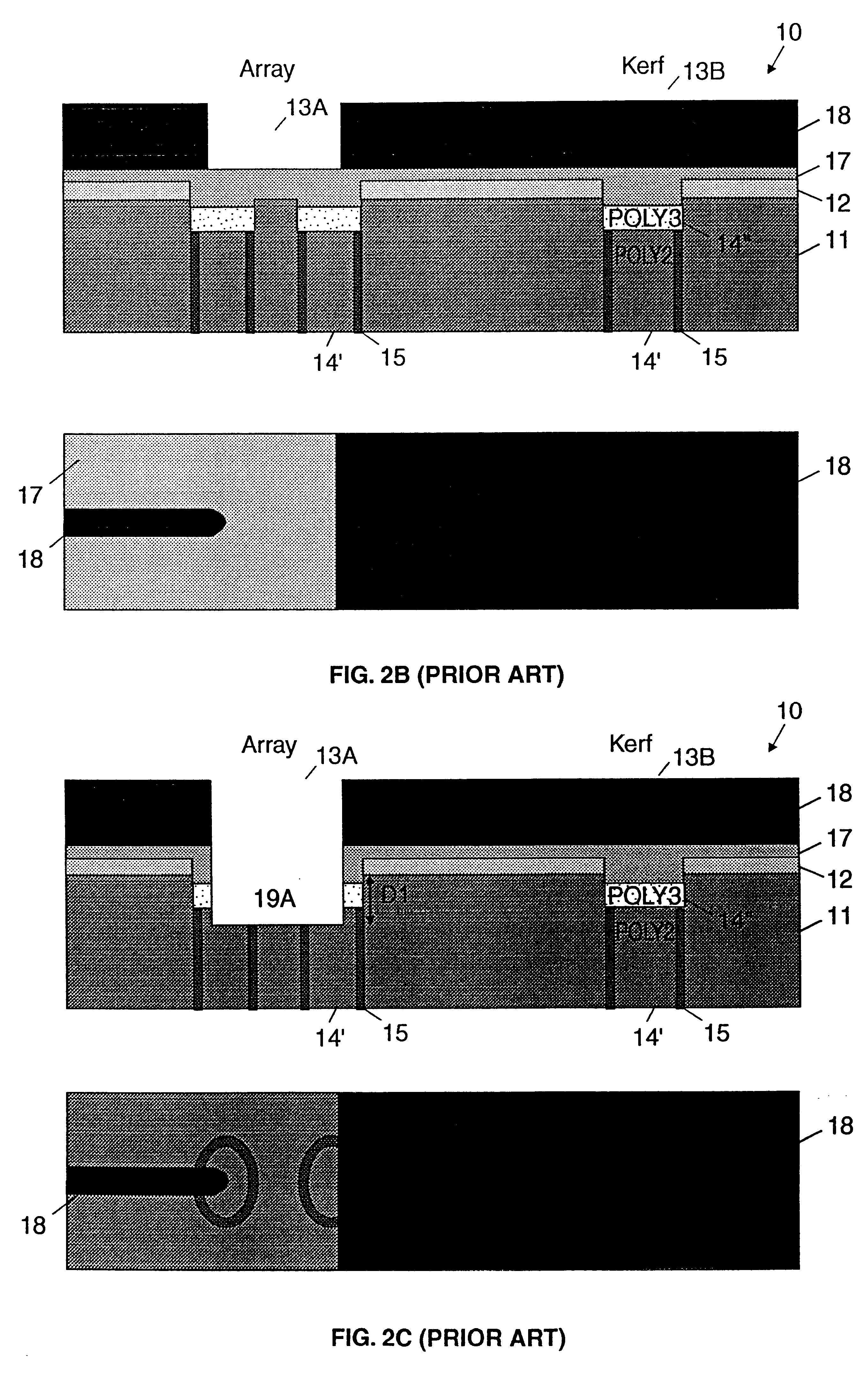
The above conventional method described by reference to FIGS. 2A-2I which requires two masking steps and which creates only recesses to be used as alignment marks is not satisfactory from a manufacturing point of view.
The KV masking step negatively affects both the cycle-time and tool capacity.
Moreover, it consumes expensive photoresist materials and necessitates the fabrication of a specific reticle increasing thereby the overall manufacturing costs.

Method used


Image

  • Method of forming STI oxide regions and alignment marks in a semiconductor structure with one masking step
  • Method of forming STI oxide regions and alignment marks in a semiconductor structure with one masking step
  • Method of forming STI oxide regions and alignment marks in a semiconductor structure with one masking step

Examples


Embodiment Construction

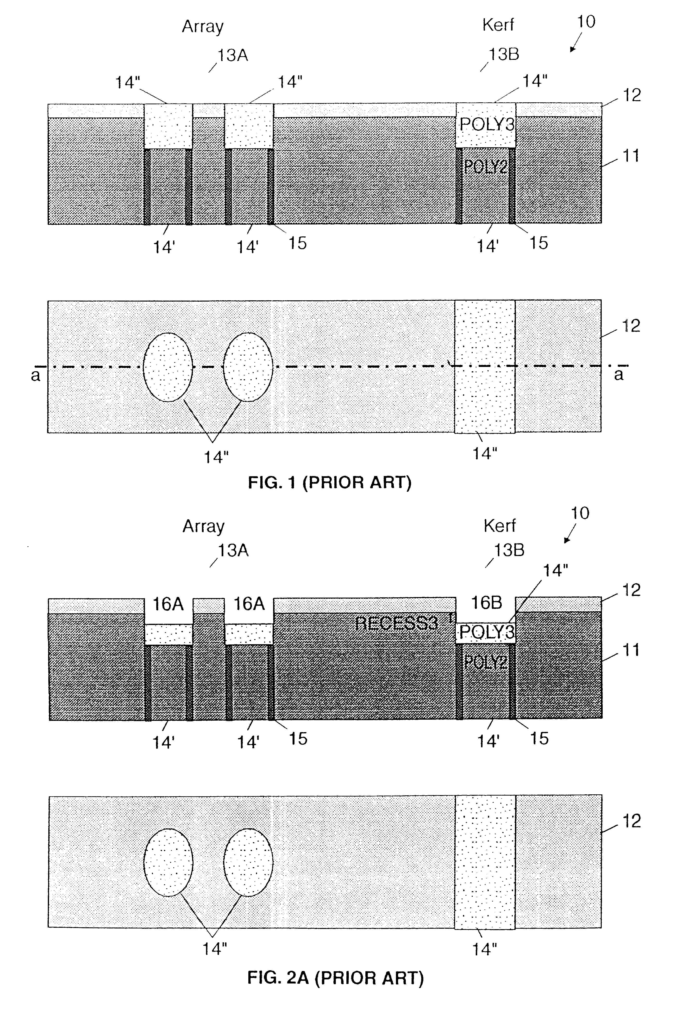
Applicant's inventors have discovered that the process flow of the prior art method described above by reference to FIGS. 2A-2I could be significantly improved. The novel method of forming the STI oxide regions and alignment marks in a semiconductor structure with only one masking step (instead of two) will be now described by reference to FIGS. 3A-3H. With regards to FIGS. 2A-2I, like reference numerals (with prime) are used through the several drawings to designate identical (corresponding) parts. The starting structure is still structure 10 shown in FIG. 1. It is important to point out that the illustrations are not necessarily drawn to scale. Basically, the essential point of the improved method consists in changes in the AA / STI step which now includes the RECESS3 etch.

First of all, according to the present invention, the AA mask is formed onto structure 10 before etching the POLY3 down to RECESS3 depth. As a consequence, it is now formed onto a planar surface which ensures a be...


PUM


Abstract

The method of the present invention applies to any semiconductor structure provided with polysilicon filled deep trenches formed in a silicon substrate coated by a Si3N4 pad layer both in the "array" and "kerf" areas. First, a photoresist mask is formed onto the structure and patterned to expose the deep trenches only in the "array" areas. Deep trenches are then anisotropically dry etched to create recesses having a determined depth. Next, the photoresist mask is removed only in the "array" areas. A step of anisotropic dry etching is now performed to extend said recesses down to the desired depth to create the shallow isolation trenches. The photoresist mask is totally removed. A layer of oxide (STI oxide) is conformally deposited by LPCVD onto the structure to fill said shallow isolation trenches in excess. The structure is planarized to create the STI oxide regions and expose deep trenches in the "kerf" areas. The polysilicon in these deep trenches is partially or totally removed by etching. Finally, the Si3N4 pad layer is eliminated, creating recesses that will be used as alignment marks for the subsequent photolithography steps. If the polysilicon is not etched, the above method will produce polysilicon bumps instead that can be used for the same purpose.

Description

The present invention relates to the manufacture of semiconductor integrated circuits and more particularly to a method of forming the STI oxide regions and alignment marks in a semiconductor structure provided with polysilicon filled deep trenches with only one masking step. STI (Shallow Trench Isolation) oxide regions are used to isolate devices from each other in the substrate and alignments marks are used in photolithography steps for reticle registration. The method finds extensive application in the field of DRAM (Dynamic Random Access Memory) and EDRAM (Embedded DRAM) chips where polysilicon filled deep and shallow trenches are formed in the semiconductor substrate.In the manufacture of semiconductor integrated circuits and especially in DRAM / EDRAM chips having polysilicon filled deep and shallow trenches formed in a silicon substrate, a specific MUV photolithography mask is used to create the alignment marks in the silicon structure that are required for reticle registration...

Claims


Application Information

Patent Timeline
Patent Type & Authority Patents(United States)
IPC IPC(8): H01L21/762H01L21/70
CPCH01L21/76232
Inventor CORONEL, PHILIPPEMACCAGNAN, RENZOLACOMBE, PHILIPPE
Owner IBM CORP
Learn More