
High-speed memory storage unit for a multiprocessor system having integrated directory and data storage subsystems

a multiprocessor system and data storage technology, applied in the field of memory units, can solve the problems of increasing complexity of data processing systems, increasing the cost of memory storage, and increasing the complexity of processors, so as to achieve less complex overall memory design, less expensive design, construction, and testing.

Inactive Publication Date: 2002-07-02
UNISYS CORP
View PDF13 Cites 83 Cited by
  • Summary
  • Abstract
  • Description
  • Claims
  • Application Information

AI Technical Summary

Benefits of technology

Each of the Data Storage Arrays 420 interfaces to the bi-directional Data Bus 340A which also interfaces with the MDA 330. Each of the Data Storage Arrays further receives selected ones of the address signals shown collectively as Address Line 370A driven by the MCA 350. As discussed above, Address Line 370A includes two unidirectional Address Buses 440 (shown as 440A and 440B), one for a pair of MSU Expansions 410. Data Storage Arrays 420A and 420C receive Address Bus 440A, and Data Storage Arrays 420B and 420D receive Address Bus 440B. This dual address bus structure allows multiple memory transfer operations to be occurring simultaneously to each of the Data Storage Arrays within an MCL 335, thereby allowing the slower memory access rates to more closely match the data transfer rates achieved on Data Buses 340.

Problems solved by technology

Data processing systems are becoming increasing complex.
Otherwise, the memory becomes a bottle neck, the processors may spend large amounts of time idle while waiting for memory requests to be processed.
This problem becomes greater as the number of processors sharing the same memory increases.
Maintaining cache coherency becomes more difficult as more caches are added to the system since more copies of a single data item may have to be tracked.
That is, if an updated copy of data existed within a local cache, other processors were prohibited from obtaining a copy of the data from main memory until the updated copy was returned to main memory, thereby releasing the lock.
For complex systems, the additional hardware and / or operating time required for setting and releasing the locks within main memory becomes too large a burden on through-put to be acceptable.
Furthermore, reliance on such locks directly prohibits certain types of applications such as parallel processing.
These snooping protocols increase processor overhead, and are unworkable in hierarchical memory configurations that do not have a common bus structure.
The Mathur snooping protocol removes some of overhead associated with snooping by invalidating data within the local caches at times when data accesses are not occurring; however, the Mathur system is still unworkable in memory systems without a common bus structure.
Such an approach is impractical for distributed systems having many caches interconnected in a hierarchical fashion because the time requited to route the invalidation requests poses an undue overhead.
Implementing high-speed memory systems that are capable of supporting a directory-based coherency protocol is problematic for several reasons.
Thus, another data access may not be initiated until the associated read-modify-write operation is complete and memory throughput is therefore diminished.
This creates practical problems.
Because SRAM devices are not as dense as DRAMs, a disproportionally large amount of circuit board area is consumed to implement the directory storage.
Moreover, SRAMs and DRAMs have different power and other electrical considerations, adding to the complexity associated with designing, placing, and routing an operational printed circuit card.
Additionally, two types of RAM devices must be stocked, then handled during the board-build process making fabrication of the printed circuit card a more difficult and expensive process.
Implementing both the directory and data memory arrays using the same logic is practically much more desirable, but would result in a decrease in overall system throughput.
Another problem associated with memory systems capable of supporting directory-based coherency protocols is that such systems tend to under-utilize shared bus resources.
After the directory state information is read, and while it is being modified by the control logic, the address, data, and control buses are idle, and bandpass is essentially wasted.
This intermittent pattern of bus usage can result in address and data buses that are idle as much as fifty percent of the time.

Method used


Image

  • High-speed memory storage unit for a multiprocessor system having integrated directory and data storage subsystems
  • High-speed memory storage unit for a multiprocessor system having integrated directory and data storage subsystems
  • High-speed memory storage unit for a multiprocessor system having integrated directory and data storage subsystems

Examples


Embodiment Construction

System Platform

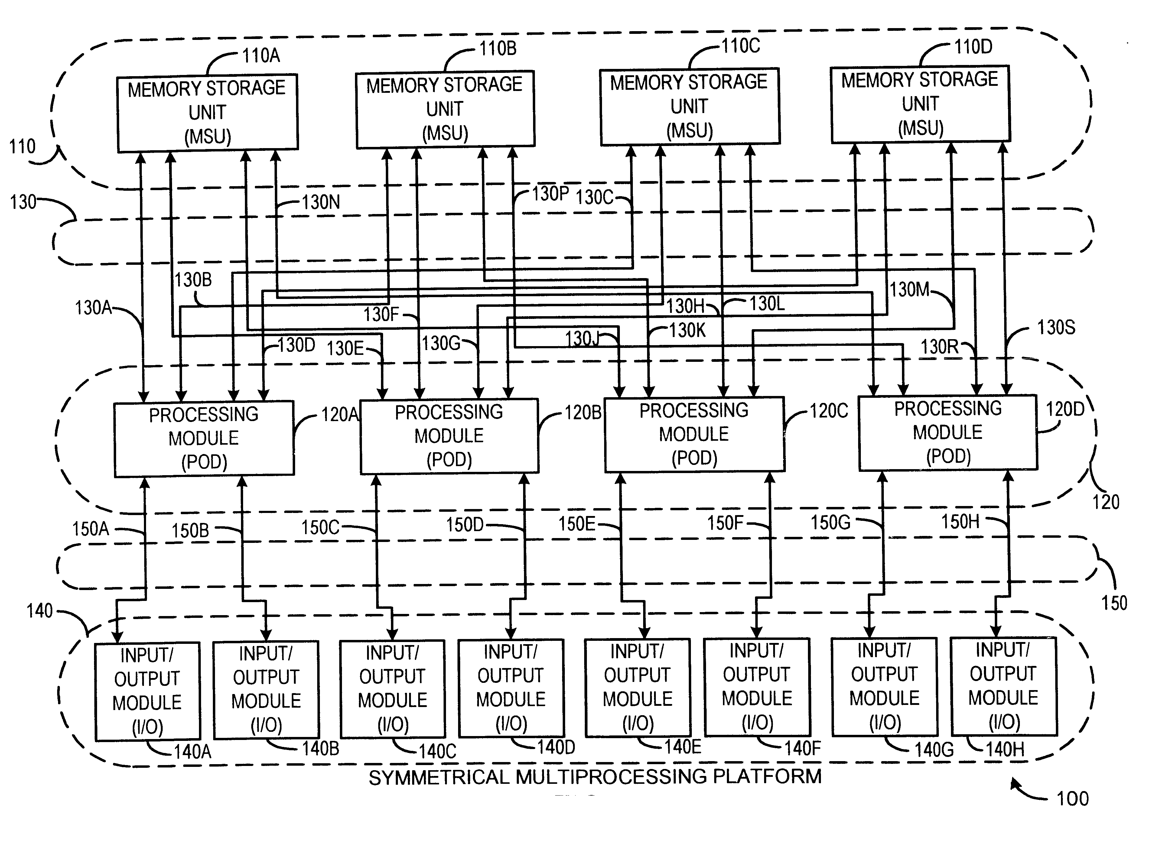
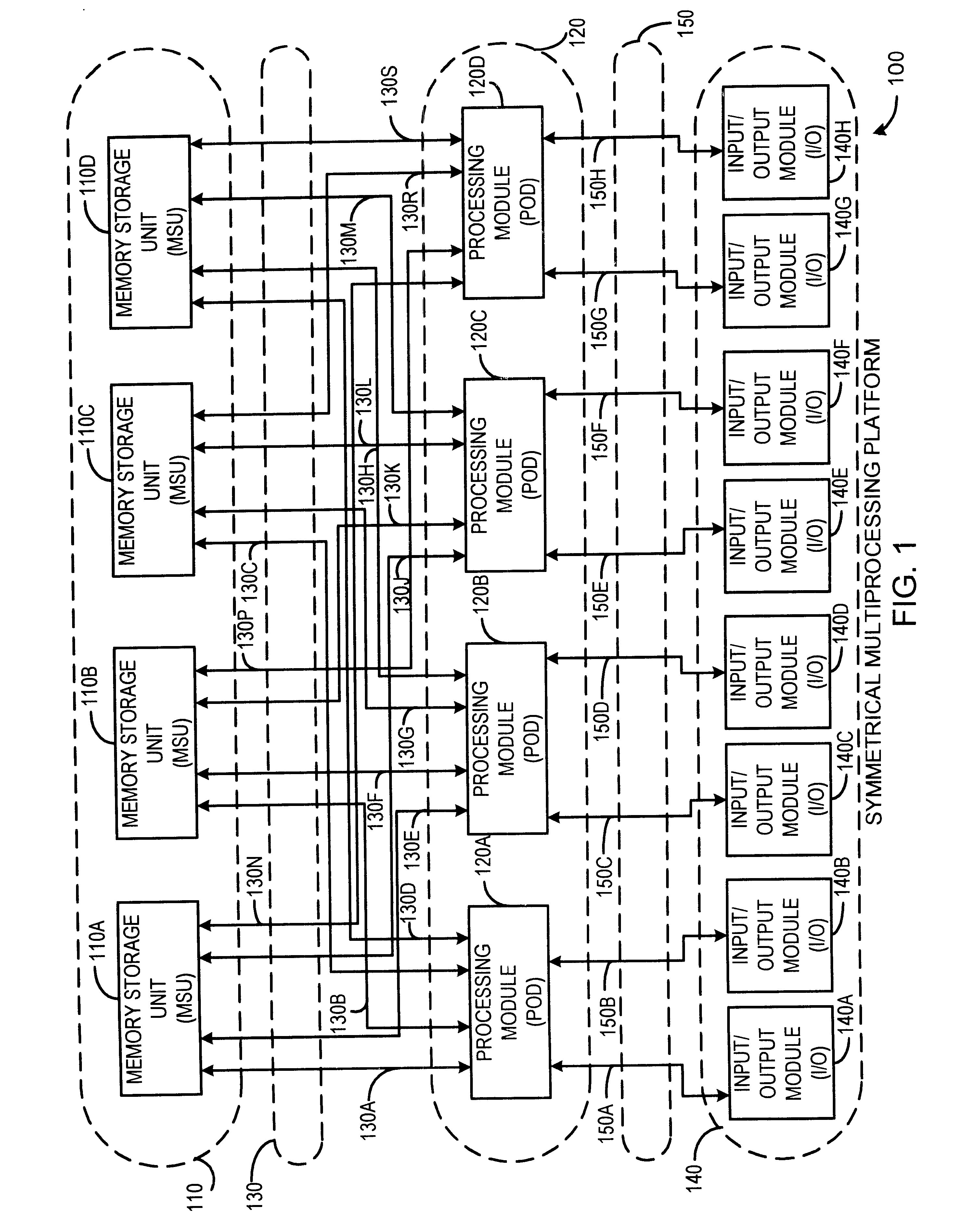
FIG. 1 is a block diagram of a Symmetrical Multi-Processor (SMP) System Platform according to a preferred embodiment of the present invention. System Platform 100 includes one or more Memory Storage Units (MSUs) in dashed block 110 individually shown as MSU 110A, MSU 110B, MSU 110C and MSU 110D, and one or more Processing Modules (PODs) in dashed block 120 individually shown as POD 120A, POD 120B, POD 120C, and POD 120D. Each unit in MSU 110 is interfaced to all units in POD 120 via a dedicated, point-to-point connection referred to as an MSU Interface (MI) in dashed block 130, individually shown as 130A through 130S. For example, MI 130A interfaces POD 120A to MSU 110A, NE 130B interfaces POD 120A to MSU 110B, MI 130C interfaces POD 120A to MSU 110C, MI 130D interfaces POD 120A to MSU 110D, and so on.

In one embodiment of the present invention, MI 130 comprises separate bi-directional data and bi-directional address / command interconnections, and further includes unidi...


PUM


Abstract

A high-speed memory system is disclosed for use in supporting a directory-based cache coherency protocol. The memory system includes at least one data system for storing data, and a corresponding directory system for storing the corresponding cache coherency information. Each data storage operation involves a block transfer operation performed to multiple sequential addresses within the data system. Each data storage operation occurs in conjunction with an associated read-modify-write operation performed on cache coherency information stored within the corresponding directory system. Multiple ones of the data storage operations may be occurring within one or more of the data systems in parallel. Likewise, multiple ones of the read-modify-write operations may be performed to one or more of the directory systems in parallel. The transfer of address, control, and data signals for these concurrently performed operations occurs in an interleaved manner. The use of block transfer operations in combination with the interleaved transfer of signals to memory systems prevents the overhead associated with the read-modify-write operations from substantially impacting system performance. This is true even when data and directory systems are implemented using the same memory technology.

Description

1. Field of the InventionThis invention relates generally to memory units within a large scale symmetrical multiprocessor system, and, more specifically, to a high-performance memory having integrated directory and data subsystems that allow for the interleaving of memory requests to a single memory unit.2. Description of the Prior ArtData processing systems are becoming increasing complex. Some systems, such as Symmetric Multi-Processor (SMP) computer systems, couple two or more processors to shared memory. This allows multiple processors to operate simultaneously on the same task, and also allows multiple tasks to be performed at the same time to increase system throughput.Although multi-processor systems with a shared main memory may allow for increased throughput, substantial design challenges must be overcome before the increased parallel processing capabilities may be leveraged. For example, the various processors in the system must be able to access memory in a timely fashion...

Claims


Application Information

Patent Timeline
Patent Type & Authority Patents(United States)
IPC IPC(8): G06F12/08
CPCG06F12/0817
Inventor BAUMAN, MITCHELL A.RODI, EUGENE A.
Owner UNISYS CORP
Learn More