
Method of anisotropic etching of substrates

a substrate and anisotropic technology, applied in the direction of basic electric elements, semiconductor/solid-state device manufacturing, electric devices, etc., can solve the problems of inevitable loss of anisotropy of etching, depletion of ions and radicals, random direction of ion movement, etc., to enhance the treatment of the silicon surface being etched, high aspect ratio, and high rate

Inactive Publication Date: 2002-05-07
WSOU INVESTMENTS LLC
View PDF20 Cites 18 Cited by
  • Summary
  • Abstract
  • Description
  • Claims
  • Application Information

AI Technical Summary

Benefits of technology

This method achieves a high etch rate and selectivity with improved uniformity and reduced mask degradation, maintaining anisotropy and stability through controlled ion directionality and constant gas flow, enhancing the manufacturing of microelectromechanical systems and microelectronics.

Problems solved by technology

Problems occur when, to increase the speed of silicon removal (i.e., the etch rate), one tries to enhance the plasma density by increasing the power coupled to the plasma discharge.
However, as the power is increased more hot ions are produced and the direction of ion movement becomes more random.
The results is that more ions and radicals are depleted by the walls of the trenches, with the inevitable loss of anisotropy of the etch.
To overcome this problem, one must reduce the etch rate, resulting in the loss of the throughput.
An additional problem encountered is mask degradation.
As etch rate is reduced, etch time, and therefore mask exposure time, are increased, leading to more rapid mask degradation, i.e., reduced selectivity.
The problem with cycling different gases is that the time ratio of the etch deposition cycle depends on the speed of the gas mixtures and varies from point to point, affecting the uniformity.
Also, this method typically requires more complex hardware and controls to introduce the two different gas mixtures in cycles.

Method used


Image

  • Method of anisotropic etching of substrates
  • Method of anisotropic etching of substrates
  • Method of anisotropic etching of substrates

Examples


Embodiment Construction

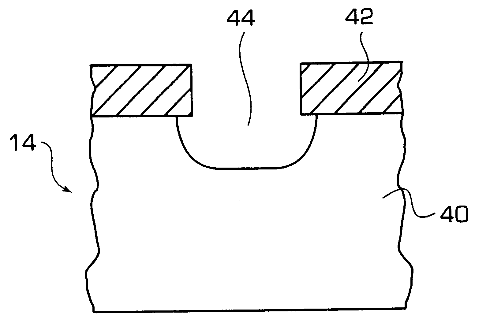
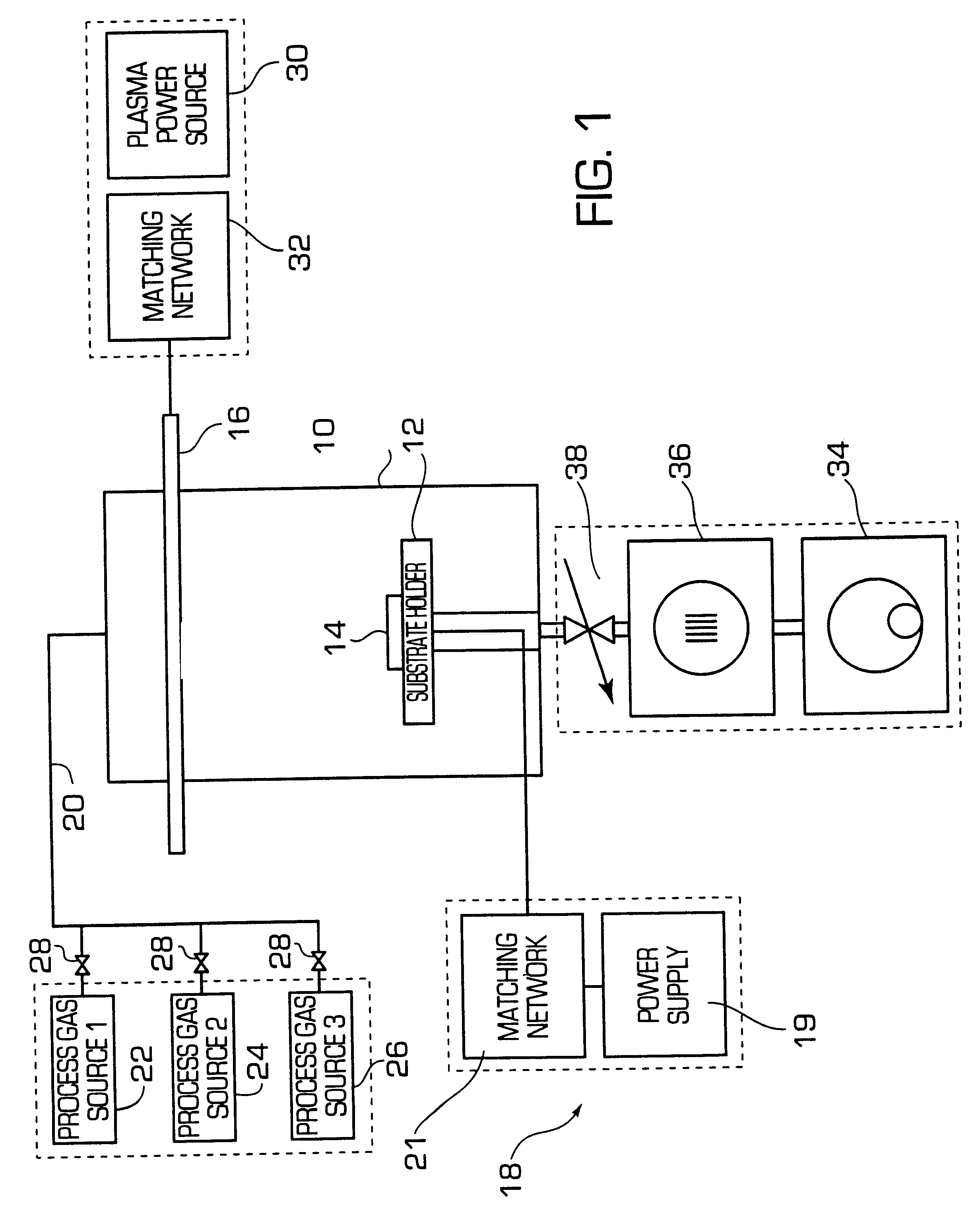
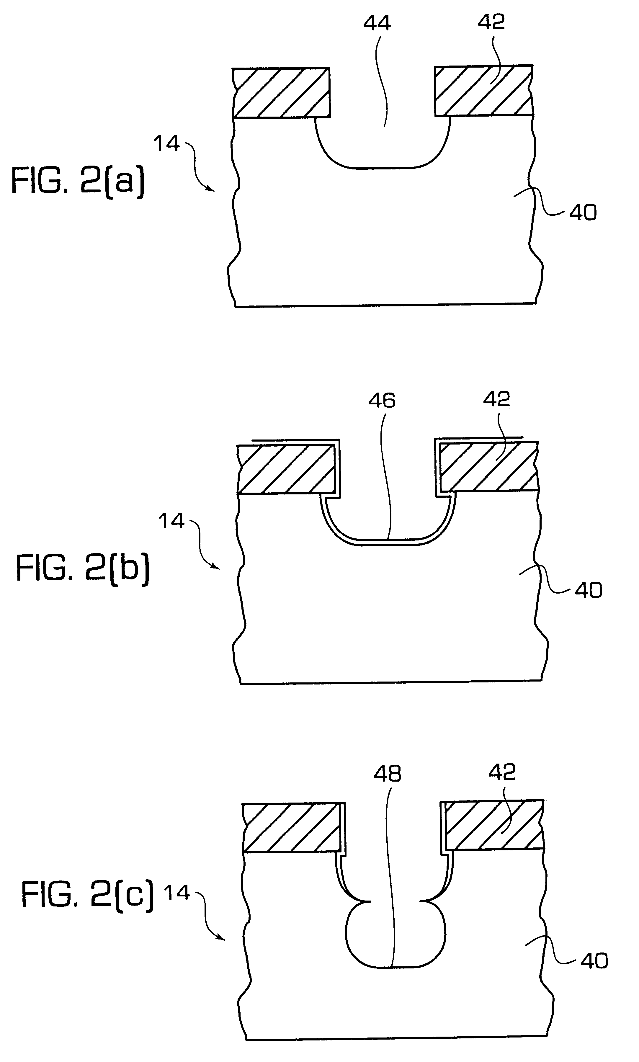
with reference to FIGS. 1 and 2(a) to 2(c). Referring to FIG. 1, the device includes an etching chamber 10. Provided within the chamber 10 is a substrate holder 12 for holding substrate 14 as well as an inductive coupler 16 provided near the top of the chamber 10. The substrate holder 12 is an electrode which is electrically connected to generator 18, including a power supply 19 and a matching network 21, for polarizing the substrate 14. Located at the top of the chamber is an inlet line 20 for introducing process gases into the chamber. The process gases are stored in gas tanks 22, 24 and 26. The flow rate of the process gases into the chamber 10 is controlled by a control valves 28. The plasma stimulation is provided by inductive coupler 16 powered by an RF power source 30 and an associated matching network 32. Pressure within the chamber 10 is controlled by mechanical pump 34, turbo-molecular pump 36 and throttle valve 38, in the conventional manner. It is of course understood th...


PUM

PropertyMeasurementUnit
gas pressureaaaaaaaaaa
poweraaaaaaaaaa
poweraaaaaaaaaa

Abstract

A method of plasma etching of silicon that utilizes the plasma to provide laterally defined recess structures through a mask. The method is based on the variation of the plasma parameters to provide a well-controlled anisotropic etch, while achieving a very high etch rate, and a high selectivity with respect to a mask. A mixed gas is introduced into the vacuum chamber after the chamber is evacuated, and plasma is generated within the chamber. The substrate's surface is exposed to the plasma. Power sources are used for formation of the plasma discharge. An integrated control system is used to modulate the plasma discharge power and substrate polarization voltage levels.

Description

1. Field of the InventionThe invention relates to a method of anisotropic plasma etching of substrates preferably defined with an etching mask in which the etch rate and selectivity is increased. The method can be well implemented for manufacturing microelectromechanical system (MEMS), as well as microelectronic devices.2. Background of the Related ArtAnisotropic plasma etching, particularly for single crystal silicon, can work independent of crystal orientation of the substrate or doping level. This method also applies to doped or undoped polysilicon. Preferred fields of applications are MEMS technology, where structures have a high aspect ratio, i.e., a high structural height to width ratio. Other examples include surface wave technology, where narrow grooves and vertical walls are etched to produce actuators, surface wave filters, delay lines, etc. Additional microelectronics applications include storage cells, insulation, collector contacts, etc.The Reactive Ion Etching (RIE) pr...

Claims


Application Information

Patent Timeline
Patent Type & Authority Patents(United States)
IPC IPC(8): H01L21/02H01L21/3065H01L21/302C23F4/00
CPCH01L21/30655
Inventor PANDHUMSOPORN, TAMARAKYU, KEVINFELDBAUM, MICHAELPUECH, MICHEL
Owner WSOU INVESTMENTS LLC
Learn More