
Structure for preventing adhesive bleed onto surfaces

a technology of adhesive and surface, applied in the direction of material nanotechnology, semiconductor devices, semiconductor/solid-state device details, etc., can solve the problems of unreceptive surface of bond pads or other metal surfaces, affecting the service life of electrical contacts, and affecting the service life of adhesives

Inactive Publication Date: 2001-06-26
GLOBALFOUNDRIES INC
View PDF9 Cites 12 Cited by
  • Summary
  • Abstract
  • Description
  • Claims
  • Application Information

AI Technical Summary

Problems solved by technology

One particular problem encountered when using such bond techniques is the tendency of the components of the epoxy adhesive to "bleed" and spread onto the wire bond surfaces, such as the wire bond pads or other noble metal surfaces, such as ground rings or voltage rings, and adhere thereto.
This "bleed" causes the surface of the bond pads or other metal surfaces to be unreceptive to the bonding of the wire bonds necessary to electrically connect the wire bond surfaces to the contacts on the I / C chip.
This, of course, results in unsatisfactory electrical contacts and, thus, contributes to an unsatisfactory chip package.
However, this is not a completely satisfactory treatment in all instances in that the fluorine containing moieties are not strongly bonded to the gold but are only lightly adhered thereto.
Therefore, they can be easily removed with organic solvents during processing before attachment of the I / C chip takes place, but not easily removed with aqueous systems during processing.
Moreover, the CF.sub.4 plasma tends, in many cases, to adversely affect the dielectric material for subsequent application of encapsulating material.

Method used


Image

  • Structure for preventing adhesive bleed onto surfaces
  • Structure for preventing adhesive bleed onto surfaces
  • Structure for preventing adhesive bleed onto surfaces

Examples


Embodiment Construction

)

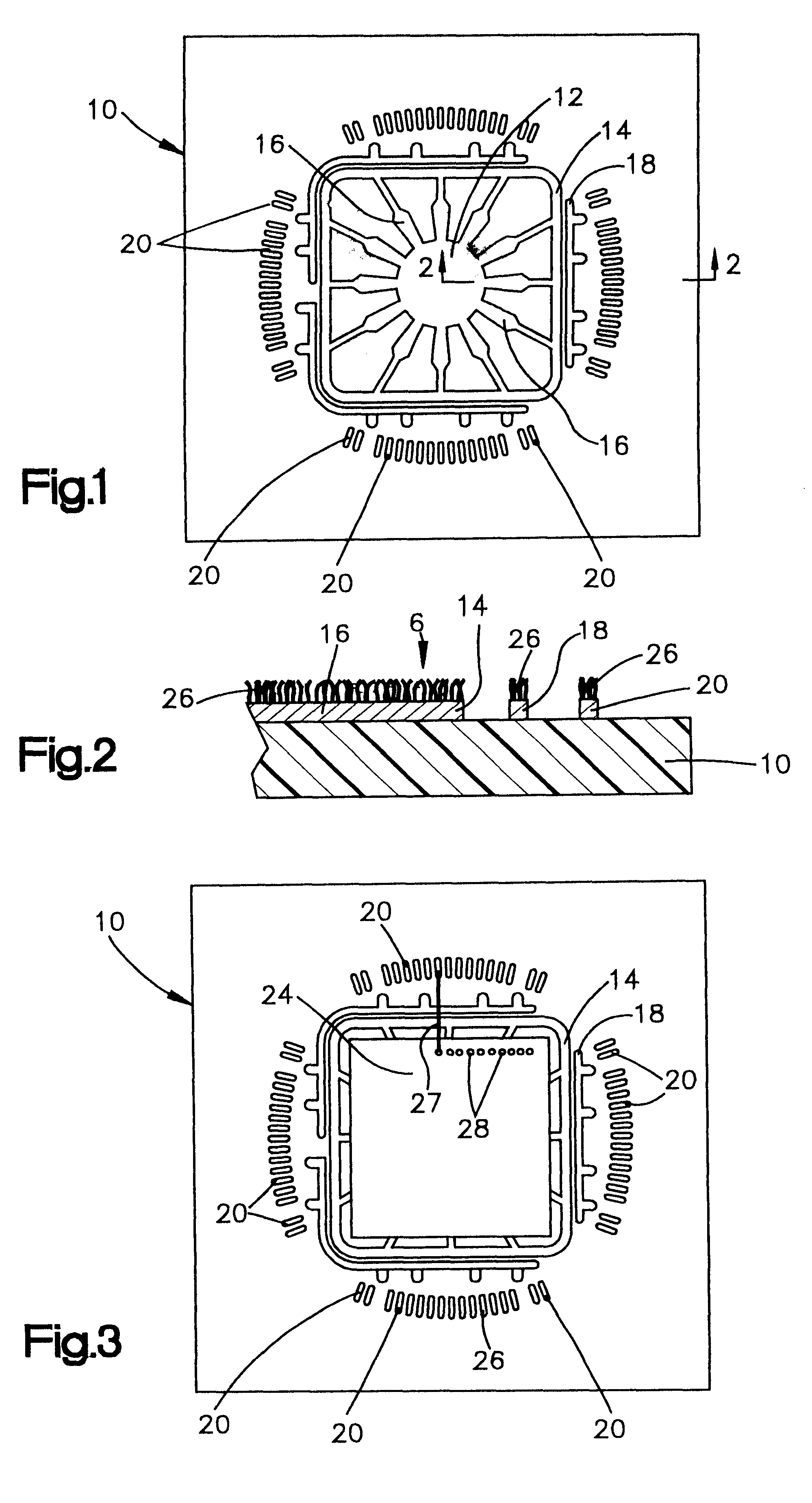
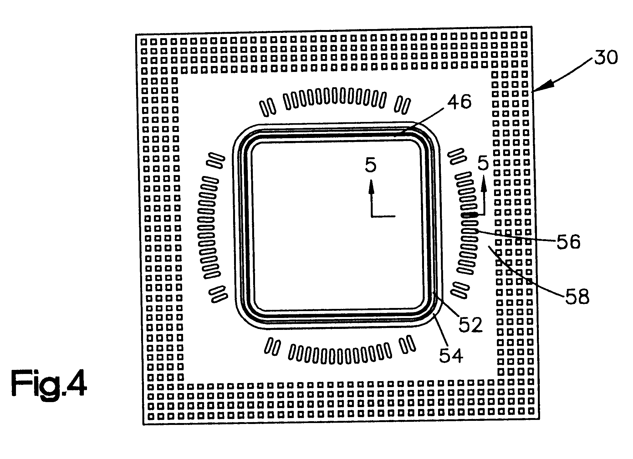
Referring now to the drawings, and, for the present, to FIG. 1, a planar chip carrier for use in the present invention is shown. The chip carrier includes an organic dielectric substrate 10 which has formed thereon a central die attach pad 12 which is connected to a ground ring 14 by fingers 16. A voltage or power ring 18 is also provided, as well as wire bond pads 20 on the surface of the substrate 10. All of the central die pad 12, ground ring 14, fingers 16, voltage or power ring 18, and wire bond pads 20, preferably are formed of gold, although other noble metals, such as palladium, platinum or silver, may be used in some instances. However, gold is the preferred material for these structures.

To attach an I / C chip or die 24 (FIGS. 3), an adhesive (not shown) is applied to the surface of the central die attach pad 12, and the die 24 is then mounted to the central die attach pad 12. A particularly useful adhesive for attaching the die 24 is a two part epoxy adhesive, such as Able...


PUM

PropertyMeasurementUnit
surface tensionaaaaaaaaaa
temperatureaaaaaaaaaa

Abstract

A method and structure is provided for preventing wetting or bleed of an adhesive, such as an epoxy, onto noble metal wire bond pads on the surface of a dielectric substrate when attaching an I / C chip to the substrate. The method includes treating the wire bond pads with a chemical composition which prevents bleeding onto the surfaces of the wire bond pads by a component of the epoxy. The chemical composition is a chemical which will provide "Self-Assembled Monolayers" (SAMs) on the surface of the gold. These compositions are characterized by a molecule having at least one group, such as a mercaptan or disulfide, connected to a hydrocarbon moiety, such as a (CH2)x chain. The affinity of the thiol or sulfur-containing portion of the molecule chemically bonding with the noble metal provides a relatively strong attachment of the molecule to the metal surface. The hydrocarbon segment presents a surface on the noble metal that has the characteristics of the hydrocarbon portion of the molecule which has a low surface tension, and, thus, prevents wetting of the noble metal by an epoxy adhesive component.The SAMs, once they provide protection from the bleed of the die attach adhesives, self desorb during the wire bonding or soldering temperatures.

Description

1. Field of the InventionThis invention relates generally to the prevention of bleeding of organic material onto a metal substrate and, more particularly, to preventing bleeding of adhesive or components thereof onto a noble metal substrate. In even more particular aspects, this invention relates to the prevention of the bleeding of any components of a die attach adhesive onto noble metal circuitry on a dielectric substrate and, specifically, onto gold wire bond surfaces on a chip carrier or other noble metal circuitry on an I / C chip mounting substrate.2. Background InformationIn the mounting of integrated circuit (I / C) chips on substrates having electrical connections, such as wire bond pads thereon, one technique of mounting utilizes a two-part epoxy adhesive to bond the chip either to gold plating on a planar surface of a substrate, or onto copper or some dielectric material in a cavity formed in an electrical substrate, which substrate also has electrical contacts or wire bond s...

Claims


Application Information

Patent Timeline
Patent Type & Authority Patents(United States)
IPC IPC(8): H01L21/02H01L21/48H01L23/498H01L23/48H01L21/607
CPCB82Y10/00B82Y30/00H01L21/4864H01L23/49894H01L24/80H01L2924/01029H01L2924/01046H01L2924/01078H01L2924/01079H01L2924/14H01L2924/01006H01L2924/01033H01L2924/01047H01L2924/01087H01L2924/014
Inventor APPELT, BERND K.JOHANSSON, GARY A.JONES, GERALD W.MATIENZO, LUIS J.NGUYEN, YENLOAN H.PAPATHOMAS, KONSTANTINOS I.
Owner GLOBALFOUNDRIES INC
Learn More