
Method of aligning nanowires

a nanowire and nanowire technology, applied in nanoinformatics, instruments, nanostructure manufacturing, etc., can solve the problems of limiting the progress of lithographically defined patterning, degrading devices, and need for increasingly finer wires

Inactive Publication Date: 2001-06-19
SAMSUNG ELECTRONICS CO LTD
View PDF5 Cites 228 Cited by
  • Summary
  • Abstract
  • Description
  • Claims
  • Application Information

AI Technical Summary

Problems solved by technology

With the constantly decreasing feature sizes of integrated-circuit devices, the need for increasingly fine, lithographically-defined patterning is limiting further advances of the technology.
However, Au and Fe migrate into Si rapidly and create deep levels, which can degrade devices, such as addressing circuitry and other portions of the system formed by conventional Si integrated-circuit technology.

Method used


Image

  • Method of aligning nanowires
  • Method of aligning nanowires

Examples


example

1. Nucleation of Silicon Nanowires on Titanium Islands on Silicon Substrates

Ti-containing islands were formed by chemical vapor deposition (CVD) on 150-mm diameter, Si(001) and Si(111) substrates in a commercially available, lamp-heated, single-wafer reactor using TiCl.sub.4 in argon as the precursor for the Ti and a H.sub.2 ambient. The partial pressure of TiCl.sub.4 was 0.06 pa (4.5.times.10.sup.-4 Torr), and the total reactor pressure was 670 pa (5 Torr). Although the Ti deposition process is selective, unpatterned wafers were used in this demonstration. In most cases, only TiCl.sub.4 was introduced from the gas phase, with the Si being supplied from the Si substrate. In a few cases, a Si-containing gas (SiH.sub.4 or SiH.sub.2 Cl.sub.2) was added during the deposition of the Ti to minimize consumption of the Si substrate during TiSi.sub.2 formation. At the low deposition temperatures of 640.degree. to 670.degree. C. used, the islands are likely to be Ti-rich compared to TiSi.sub....


PUM

PropertyMeasurementUnit
ion energyaaaaaaaaaa
timeaaaaaaaaaa
timeaaaaaaaaaa

Abstract

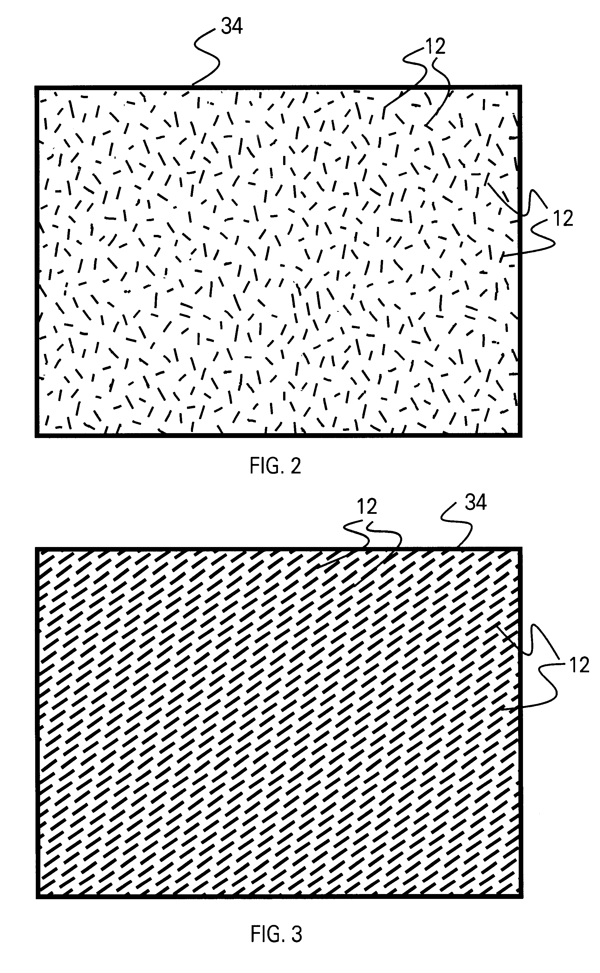
A method of aligning nanowires on a substrate is provided. First, a plurality of the nanowires is formed on the substrate, then the plurality of nanowires is exposed to a flux of energetic ions, e.g., argon at an ion energy of 5 KV and an integrated flux density of about 6x10¹⁵ ions / cm2. The flux of energetic ions serves to align the nanowires parallel to each other. The flux of energetic ions may also be used to align the nanowires parallel to the substrate surface.

Description

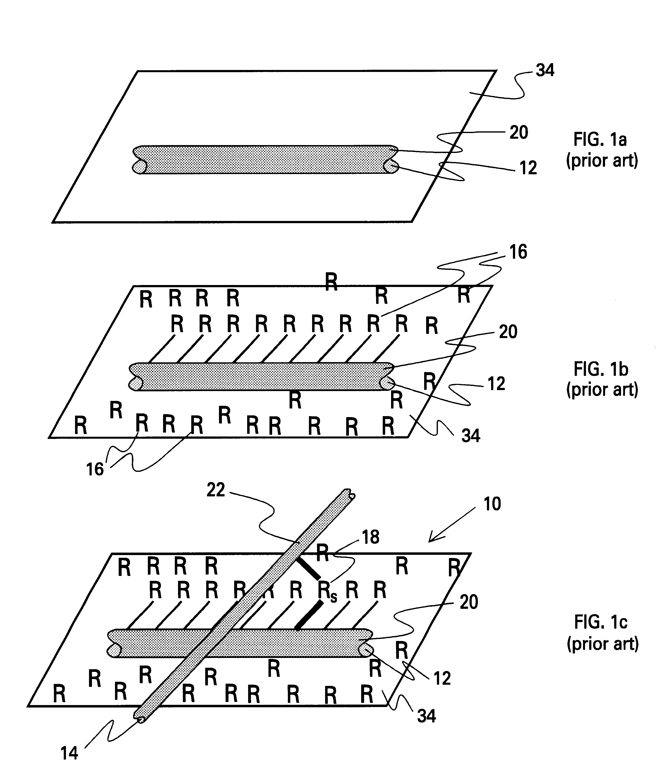
The present application is generally directed to nanoscale computing and memory circuits, and, more particularly, to the formation of nanowires for device applications, specifically, to the alignment of such nanowires.With the constantly decreasing feature sizes of integrated-circuit devices, the need for increasingly fine, lithographically-defined patterning is limiting further advances of the technology. Consequently, a growing amount of effort is being devoted to self-assembly techniques to form switching elements without fine-scale lithography; see, e.g., C. P. Collier et al, "Electronically Configurable Molecular-Based Logic Gates", Science, Vol. 285, pp. 391-394 (Jul. 16, 1999). The self-assembled switching elements may be integrated on top of a Si integrated circuit so that they can be driven by conventional Si electronics in the underlying substrate. To address the switching elements, interconnections or wires, preferably also formed by self-assembly, are needed. The self-as...

Claims


Application Information

Patent Timeline
Patent Type & Authority Patents(United States)
IPC IPC(8): B82B3/00G11C13/02
CPCB82B3/00B82Y10/00B82Y30/00B82Y40/00G11C2213/81Y10S977/84H01L2924/0002H01L2924/00
Inventor KAMINS, THEODORE I.CHANG, YING-LAN
Owner SAMSUNG ELECTRONICS CO LTD
Learn More