Magnetoresistance element and its manufacture
a technology of magnetoresistance element and manufacturing method, applied in the field of magnetoresistance element, can solve the problems of large h.sub.s, insufficient mr ratio, and no clear report on the effect of oxygen concentration in each layer
- Summary
- Abstract
- Description
- Claims
- Application Information
AI Technical Summary
Benefits of technology
Problems solved by technology
Method used
Image
Examples
embodiment 1
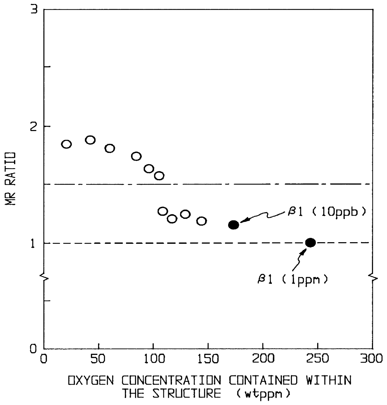
In this example, the difference in the procedure from that employed in that the attained degree of vacuum within the film formation chamber was approximately 10.sup.-7 Torr. Furthermore, the impurity concentration contained within the Ar gas was set to either 10 ppb or 1 ppm.
The other points were identical to those in embodiment 1.
The sample produced in this example is designated .beta.1 (i). Here, i indicates the impurity concentration contained in the Ar gas. In FIG. 1, the MR ratio of the magnetoresistance elements produced are indicated by a white circle (for sample .alpha.) and a black circle (for sample .beta.). The horizontal axis in FIG. 1 indicates the oxygen concentration contained within the structure comprising NiFe and Cu. The measurement of this oxygen concentration was conducted by means of SIMS. The vertical axis in FIG. 1 indicates the MR ratio as measured by means of the direct current four terminal method shown in FIG. 7; this was standardized to the 131 (1 ppm) o...
embodiment 2
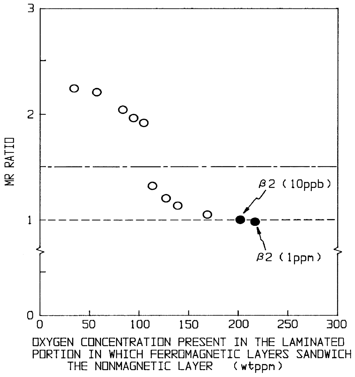
In the present embodiment, the effects will be described of limiting the oxygen concentration contained in the nonmagnetic layers, the ferromagnetic layers and the antiferromagnetic layer of a spin valve type magnetoresistance element. In order to confirm this effect, film formation was conducted such that the attained degree of vacuum within the film formation chamber was set at approximately 10.sup.-9 Torr, and the impurity concentration contained in the Ar gas used during the formation of the nonmagnetic layers and ferromagnetic layers was varied within a range of 10 ppb to 1 ppm. The nonmagnetic layer was formed from Cu, the ferromagnetic layers were formed from FeNi, and the antiferromagnetic layer was formed from FeMn.
FIG. 6(a) shows a cross-sectional view of an example of a DC magnetron sputtering device used in producing the magnetoresistance elements in the present embodiments. The inner walls of vacuum chamber 600 were subjected to compound electropolishing. Furthermore, F...
embodiment 3
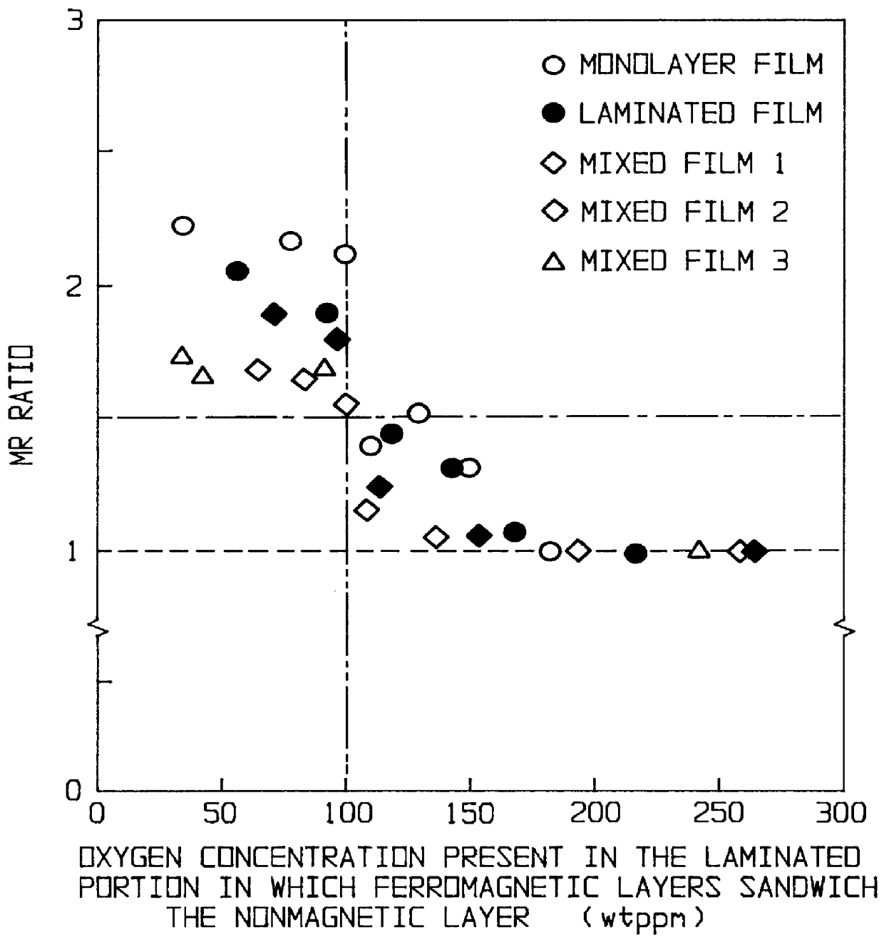
In the present embodiment, the point of difference from embodiment 2 was that a laminated film containing a Co monolayer, a NiFe film and a Co film was used as the ferromagnetic layer, and a mixed film containing the nonmagnetic elements Cu (0.3 wt %), Mo (0.3 wt %), and Nb (0.3 wt %) was used as the NiFe alloy film. The layer structure of the magnetoresistance element and the total film thickness thereof were identical to those in embodiment 2. A four cathode film formation device was employed.
The other points were identical to those of embodiment 2.
The type of ferromagnetic layer, and the layer structure thereof, are shown in Table 3.
FIG. 3 shows the experimental results of this embodiment. It can be seen from FIG. 3 that independent of the type of ferromagnetic layer, when the oxygen concentration contained within the laminated portion in which the ferromagnetic layers sandwich a nonmagnetic layer in this structure reaches a level of 100 wt. ppm. or less, then the MR ratio increa...
PUM
| Property | Measurement | Unit |
|---|---|---|
| Fraction | aaaaa | aaaaa |
| Nanoscale particle size | aaaaa | aaaaa |
| Nanoscale particle size | aaaaa | aaaaa |
Abstract
Description
Claims
Application Information
 - R&D
- Intellectual Property
- Life Sciences
- Materials
- Tech Scout
- Unparalleled Data Quality
- Higher Quality Content
- 60% Fewer Hallucinations
Browse by: Latest US Patents, China's latest patents, Technical Efficacy Thesaurus, Application Domain, Technology Topic, Popular Technical Reports.
© 2025 PatSnap. All rights reserved.Legal|Privacy policy|Modern Slavery Act Transparency Statement|Sitemap|About US| Contact US: help@patsnap.com


