
Integrated germanium photodetector with silicon nitride launch waveguide

Pending Publication Date: 2022-09-08
ALPINE OPTOELECTRONICS INC
View PDF0 Cites 0 Cited by
  • Summary
  • Abstract
  • Description
  • Claims
  • Application Information

AI Technical Summary

Benefits of technology

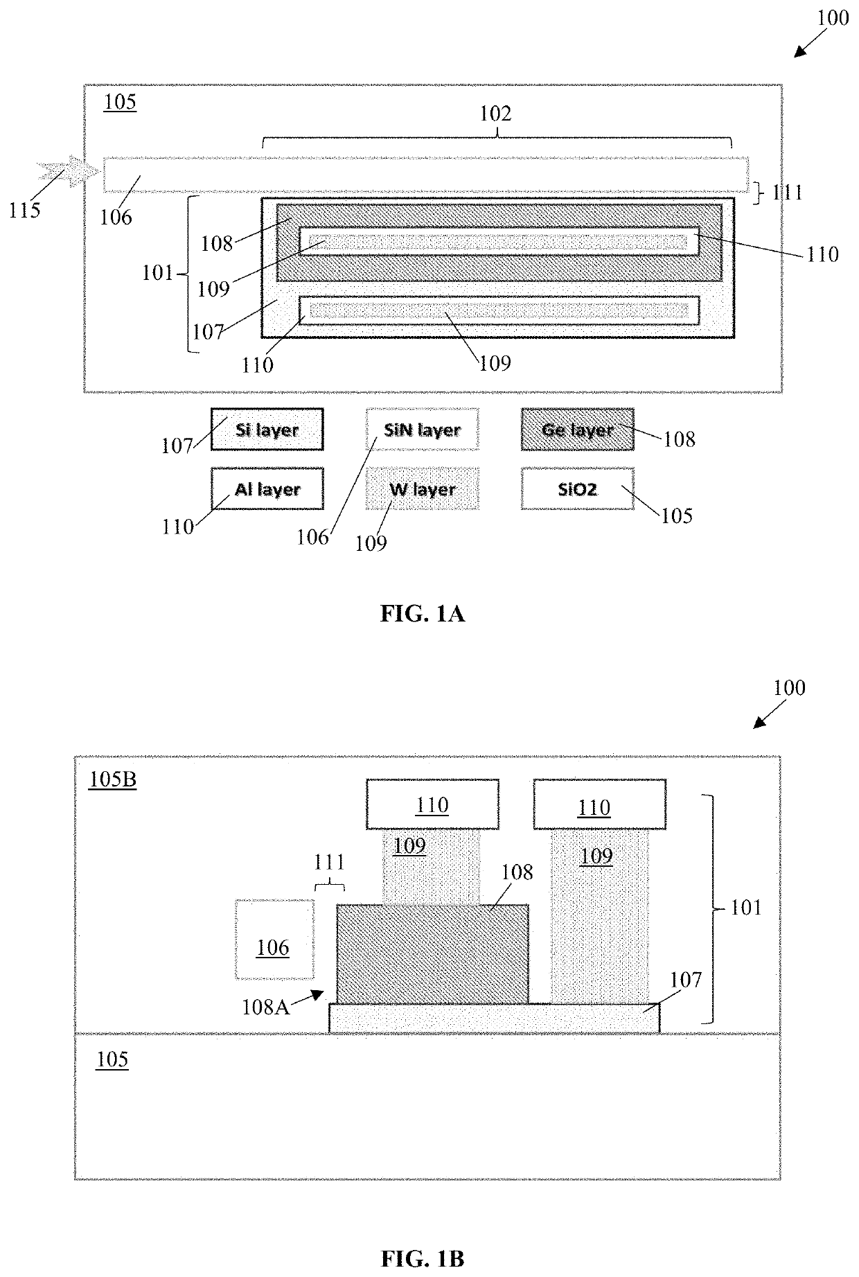
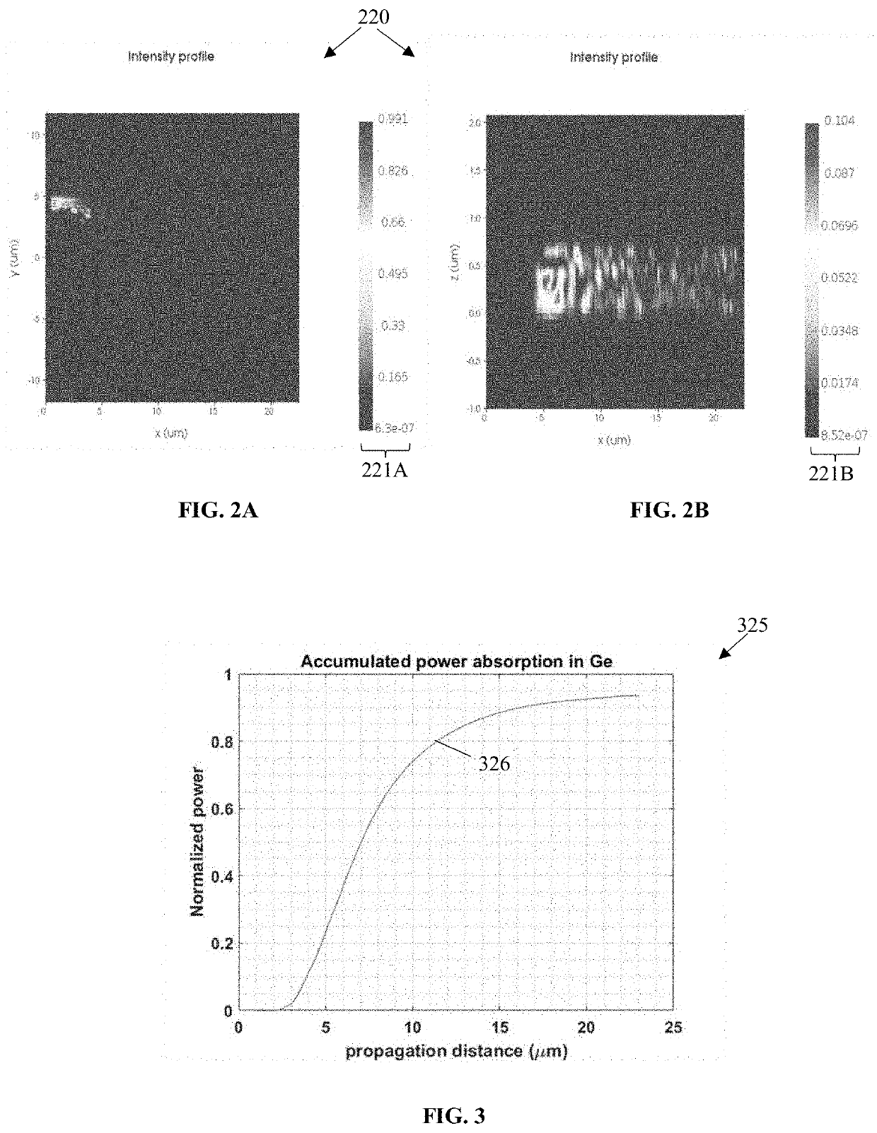
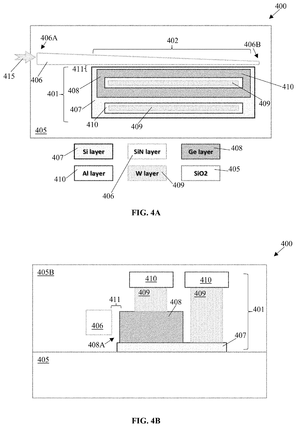
The patent describes an integrated germanium photodetector that can effectively absorb and convert optical light into an electrical signal. This is achieved by using a silicon nitride launch waveguide that enhances the optical coupling with the germanium layer. The integrated germanium photodetector has several advantages, including the ability to match polarized light group delays, lower propagation loss, and reduced dark current. Additionally, the integrated germanium photodetector can be used for visible light detection and can be evanescently coupled into both vertical and lateral integrated germanium photodetector varieties. The patent also describes a method for integrating the optical apparatus onto an optical waveguide of an integrated photonics chip.

Problems solved by technology

Moreover, this Summary is not intended for use as an aid in determining the scope of the claimed subject matter.

Method used


Image

  • Integrated germanium photodetector with silicon nitride launch waveguide
  • Integrated germanium photodetector with silicon nitride launch waveguide
  • Integrated germanium photodetector with silicon nitride launch waveguide

Examples


embodiment 800

[0060]FIGS. 8A-8B are diagrams illustrating a top view and a front elevation cross-sectional view, respectively, of an alternative embodiment of the optical apparatus 800 comprising a lateral integrated germanium photodetector 801 and a silicon nitride launch waveguide 806, according to an aspect. As described throughout this disclosure above, the integrated germanium photodetector of the present invention may be provided as either a lateral PD or a vertical PD, based on the chosen configurations of the diode implantations (not shown), the vias (e.g., 709), and the interconnected metal contacts (e.g., 710). Additionally, as disclosed herein above, the silicon nitride waveguide (e.g., 706) may be provided parallelly to a side of the germanium layer of the integrated germanium photodetector. As will be described in detail below, in an alternative embodiment 800 of the disclosed optical apparatus, a lateral Ge PD may be provided with a silicon nitride waveguide disposed above the germa...

embodiment 900

[0065]FIGS. 9A-9B are diagrams illustrating a top view and a front elevation cross-sectional view, respectively of an optical apparatus 900 comprising a lateral integrated germanium photodetector 901 and a butt-coupled silicon nitride launch waveguide 906, according to an aspect. As described throughout this disclosure above, the integrated germanium photodetector of the present invention may be provided as either a lateral PD or a vertical PD, based on the chosen configurations of the diode implantations (not shown), the vias (e.g., 809), and the interconnected metal contacts (e.g., 810). Additionally, as disclosed herein above, the silicon nitride waveguide (e.g., 706, 806) may be provided parallelly to a side or along a top of the germanium layer of the integrated germanium photodetector. As will be described in detail below, in an alternative embodiment 900 of the disclosed optical apparatus, a lateral Ge PD may be provided with a silicon nitride waveguide butt-coupled to the ge...


PUM


Abstract

An optical apparatus comprising an integrated germanium photodetector associated with a silicon nitride launch waveguide, the integrated germanium photodetector comprising a silicon layer, a germanium layer disposed atop the silicon layer, a plurality of conductive vias, at least one conductive via of the plurality of conductive vias being disposed atop the germanium layer, and a plurality of metal contacts each interconnected to each of the plurality of conductive vias; wherein the silicon nitride launch waveguide extends over a length of the silicon layer, and such that to create a coupling region between the silicon nitride launch waveguide and the germanium layer; and wherein, when an optical signal is launched into the silicon nitride launch waveguide, the optical signal is caused to be coupled into the integrated germanium photodetector at the coupling region, such that to be absorbed by the germanium layer.

Description

CROSS-REFERENCE TO RELATED APPLICATIONS[0001]This application claims the benefit of U.S. Provisional Application No. 63 / 158,286, filed Mar. 8, 2021, which is hereby incorporated by reference, to the extent that it is not conflicting with the present application.BACKGROUND OF INVENTION1. Field of the Invention[0002]The invention relates generally to integrated photodetectors on silicon photonics chips, and more specifically to integrated germanium photodetectors having a silicon nitride launch waveguide on silicon photonics chips.2. Description of the Related Art[0003]In the field of integrated silicon photonics, CMOS-compatible (i.e., compatible with the standard flow of silicon photonics foundries) integrated germanium photodetectors (Ge PDs) have been widely used and adapted for highspeed optical-to-electrical (OE) conversion, power monitoring, and many other applications. In a typical germanium photodetector, a germanium layer is epitaxially grown atop a silicon (Si) layer on a s...

Claims


Application Information

Patent Timeline
IPC IPC(8): G02B6/42H01L31/0232G02B6/293
CPCG02B6/4298H01L31/02327G02B6/4215G02B6/29344H01L31/028H01L31/022408G02B2006/12061G02B2006/12123G02B6/1228
Inventor ZHANG, XINGYUZHENG, DAWEIWANG, TONGQING
Owner ALPINE OPTOELECTRONICS INC
Learn More