
Induced crosstalk circuit for improved sensor linearity

a crosstalk circuit and linearity technology, applied in the field of optical sensors, can solve the problems of high degree of variability regarding the magnitude and induced phase shift, inevitability of crosstalk, and negligible susceptibility

Active Publication Date: 2022-07-14
YSI INC
View PDF5 Cites 0 Cited by
  • Summary
  • Abstract
  • Description
  • Claims
  • Application Information

AI Technical Summary

Benefits of technology

The present patent provides a new and unique corrective signal processing algorithm for optical sensors that can reduce or eliminate unwanted electrical interference. This algorithm combines real-time magnitude and phase information to achieve internal / self-linearity correction. The patent also describes an inductive loop that can enhance the efficacy of the correction algorithm. The invention can be used with or without an inductive loop and helps to provide optical sensors with accurate and reliable signaling.

Problems solved by technology

In the prior art, environmental sensing is up against two conflicting industry trends:1) state of the art sensor technologies are trending toward ever-smaller dimensions forcing undesirable affects such as electrical crosstalk, and2) the demand in environmental sensing is requiring ever-increasing sensitivity thereby exacerbating the problems associated with crosstalk.
The consequence: Crosstalk is an inevitability despite diligent execution of best practices in a PCB layout.
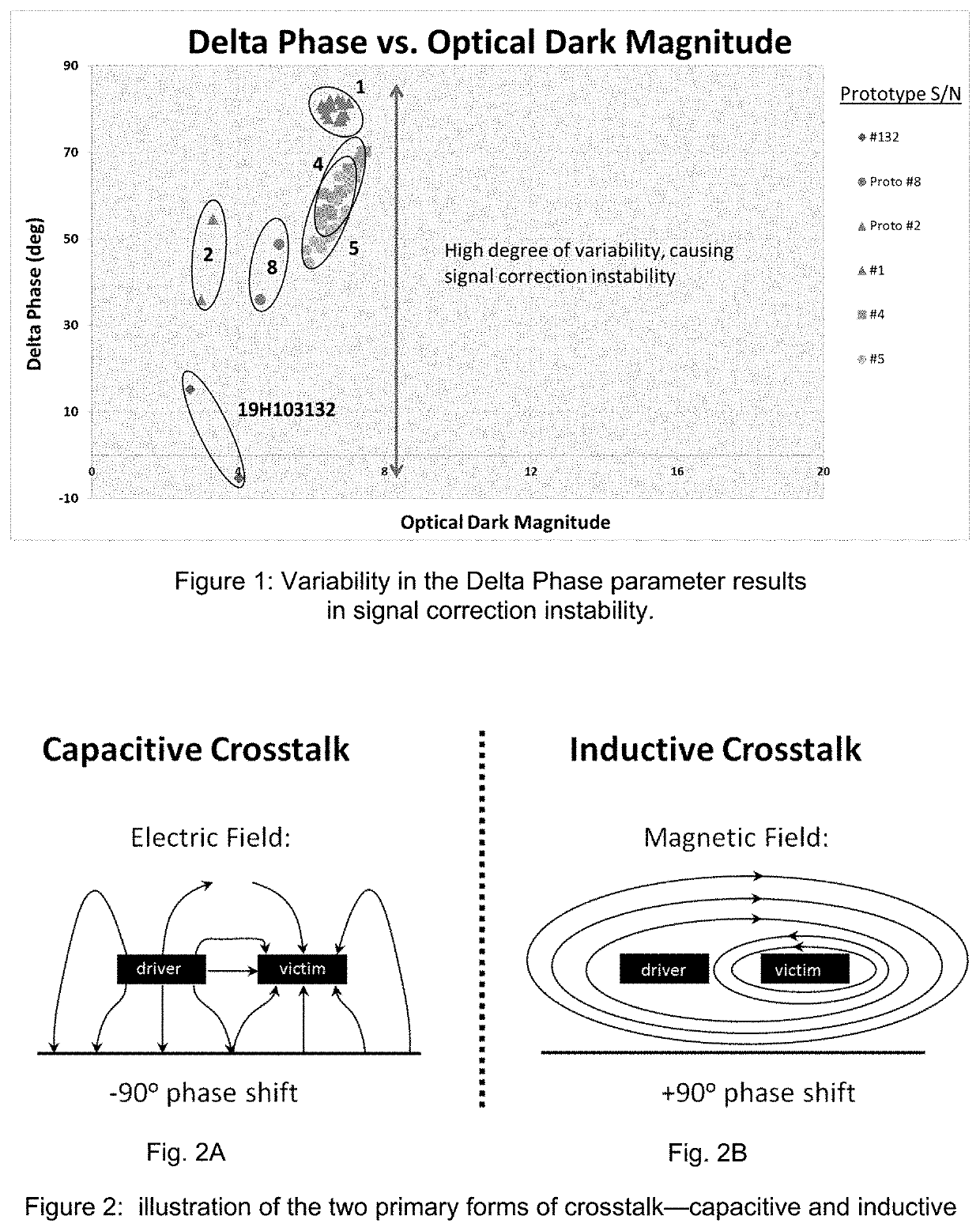
Moreover, a high degree of variability regarding the magnitude and induced phase shift stemming from the crosstalk also exists in the known sensor technologies.
Furthermore, the electrical crosstalk magnitude and phase shift are not perfectly fixed inalienable system constants impervious to the external environment, but instead demonstrate a non-negligible susceptibility to the electrical circuitry to which they interface.
Such effects have undesirable consequences regarding the efficacy of the corrective signal processing.
In particular, the signal phase, which serves as one of the signal processing inputs, is susceptible to phase noise, especially when attempting to resolve the phase of very low signal magnitudes as is often the case for electrical crosstalk signals.
While a vanishingly small crosstalk signal would be acceptable (as this would indicate a negligible electrical crosstalk), however, it is more often the case that crosstalk signals are small enough in magnitude to be susceptible to phase noise, creating a noisy corrective input, but are still large enough to impede the required signal linearity.
Finally, the variability in the induced phase shift also poses a problem.
However, for the Delta Phase, this is not the case as any change in this parameter, once set as a calibration constant, will result in an error for the correction, e.g., consistent with that set forth herein.

Method used


Image

  • Induced crosstalk circuit for improved sensor linearity
  • Induced crosstalk circuit for improved sensor linearity
  • Induced crosstalk circuit for improved sensor linearity

Examples


Embodiment Construction

Summary of the Basic Invention

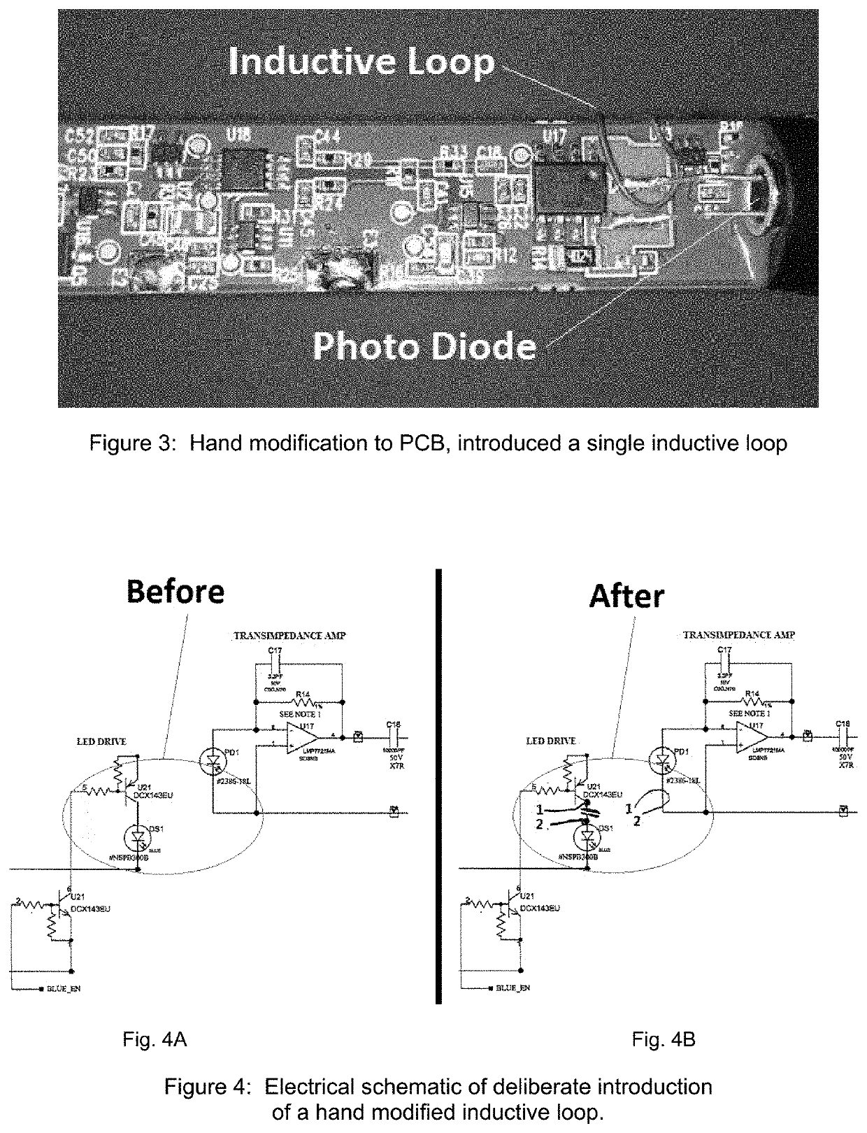
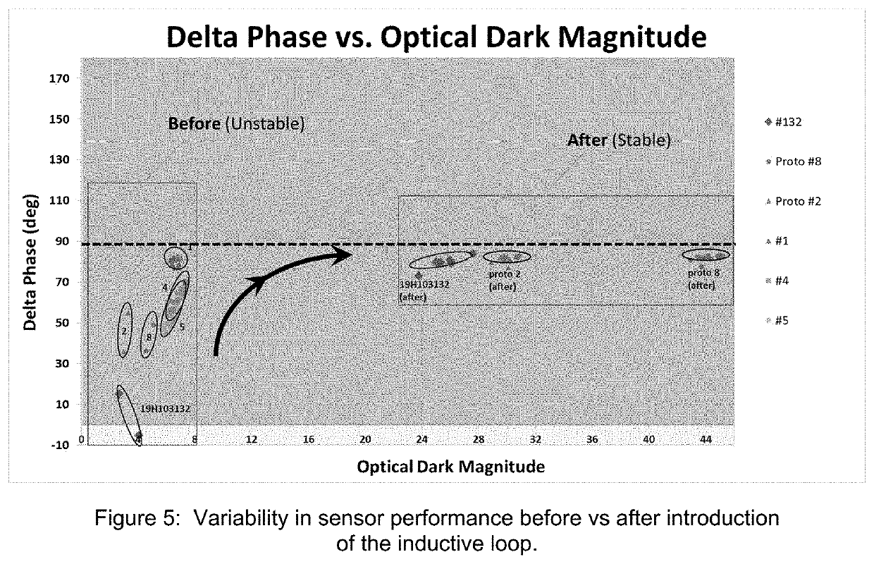
[0061]In summary, the present invention alleviates the vulnerabilities presented in the corrective signal processing algorithm by deliberately inducing a moderate inductive crosstalk with optimal phase shift at a specific location on the PCB. For example, if the crosstalk signal is sufficiently large (but not too large) in magnitude (approximately 2-5% of available analog-to-digital converter range), then the respective signal phase will be well-resolved and provide a stable input into the corrective signal processing. The question becomes: Where is the ideal location for deliberately induced crosstalk? By way of example, and according to some embodiments, the present invention provides the photodiode as an ideal location for deliberately induced crosstalk, since it is the most critical component in the receive side of the circuit (receive side—meaning any and all circuitry dedicated to receiving and propagating the electro-optical signal). The photodio...


PUM


Abstract

An optical sensor includes a detector having a printed circuit board (PCB) and an inductive loop. The printed circuit board (PCB) has a photodiode cathode pad with a photodiode. The inductive loop is arranged around at least part of the photodiode cathode pad, and configured to receive inductive loop inducing signaling, and provide inductive loop signaling around the at least part of the photodiode cathode pad to provide inductive on the PCB to reduce or substantially eliminate unwanted electrical interference in electrical photodiode signaling provided from the photodiode. The inductive loop includes a trace and at least one via. The trace has a route along a signal path from a transistor collector pin around an LED anode pad. The at least one via is placed between LED anode pads to route the trace on a top side of the PCB, and the trace is routed alongside, near and around the photodiode cathode pad back to the LED anode of the LED anode pad.

Description

CROSS-REFERENCE TO RELATED APPLICATIONS[0001]This application claims benefit to provisional patent application Ser. No. 63 / 135,799 (911-023.12-2 / N-YSI-0050US01), filed 11 Jan. 2021, which is incorporated by reference in its entirety.BACKGROUND OF THE INVENTION1. Field of Invention[0002]This invention relates to an optical sensor, such as a fluorometer; and more particularly, to an optical sensor having a printed circuit board (PCB) having a photodiode cathode pad with a photodiode.2. Description of Related Art[0003]In the prior art, environmental sensing is up against two conflicting industry trends:[0004]1) state of the art sensor technologies are trending toward ever-smaller dimensions forcing undesirable affects such as electrical crosstalk, and[0005]2) the demand in environmental sensing is requiring ever-increasing sensitivity thereby exacerbating the problems associated with crosstalk.The consequence: Crosstalk is an inevitability despite diligent execution of best practices i...

Claims


Application Information

Patent Timeline
IPC IPC(8): G01N21/64H05K1/11H05K1/18H05K1/02
CPCG01N21/64H05K1/111H05K2201/10151H05K1/0216H05K2201/10121H05K1/181G01N21/645H05K2201/10106H05K2201/1003G01N2201/12792
Inventor FLANAGAN, KEVIN R.PARMLEY, STEVEN M.POSEY, DOUGLAS J.LEISS, MICHAEL
Owner YSI INC
Learn More