Method for preparing sodium interface and method for preparing sodium-based optical structure device

Pending Publication Date: 2022-06-30
NANJING UNIV
View PDF4 Cites 0 Cited by
  • Summary
  • Abstract
  • Description
  • Claims
  • Application Information

AI Technical Summary

Benefits of technology

The present invention provides a new method for preparing a stable sodium interface, which can be used for various optical applications such as plasmon polariton optical waveguides and nano-lasers. The method allows for easy and quick preparation of a sodium interface at low cost, with the ability to adjust sample size for large-scale production. The prepared sodium interface can be stably exposed to the air for long-term operation, and a sodium-based micro-nano structure can be prepared using this method for optical device applications.

Problems solved by technology

However, these two metals suffer great optical losses in plasmon polariton application, limiting the performance of devices.
Besides, as noble metals, they are costly.
However, as it has a relatively high chemical activity, a stable and smooth metal interface and a metal micro-nano structure are difficult to prepare, and thus the application of metals in plasmon polaritons and the like are difficult to realize.
The conventional methods for preparing metal films include physical deposition and crystal growth, wherein the former has the disadvantages of high instrument cost, strict preparation conditions and long deposition time, while the latter demands a strictly controlled external environment and long growth period, and samples prepared using the two methods have limited sizes.
Therefore, the large-scale production of metal films is difficult to realize.
Moreover, due to the high chemical activity of sodium, a stable metal interface and a micro-nano structure can be formed only in an environment with extremely low oxygen concentration and water concentration, which is difficult to create using the above preparation methods.
Specifically, when the temperature of the liquid sodium is too high, the liquid sodium is very easy to separate from the substrate during the spin coating process and thus cannot form a sodium interface on the substrate, while when the temperature of the liquid sodium is too low, the viscosity is high, and the coagulation speed is low, so that a complete and uniform sodium interface cannot be obtained on the substrate.

Method used


Image

  • Method for preparing sodium interface and method for preparing sodium-based optical structure device
  • Method for preparing sodium interface and method for preparing sodium-based optical structure device
  • Method for preparing sodium interface and method for preparing sodium-based optical structure device

Examples


example 1

[0032

[0033]A smooth sodium interface was prepared by the following specific steps.

[0034]In a glove box filled with the inert gas argon, with the ambient oxygen concentration less than 20 ppm and the water concentration less than 20 ppm, the following steps were carried out:

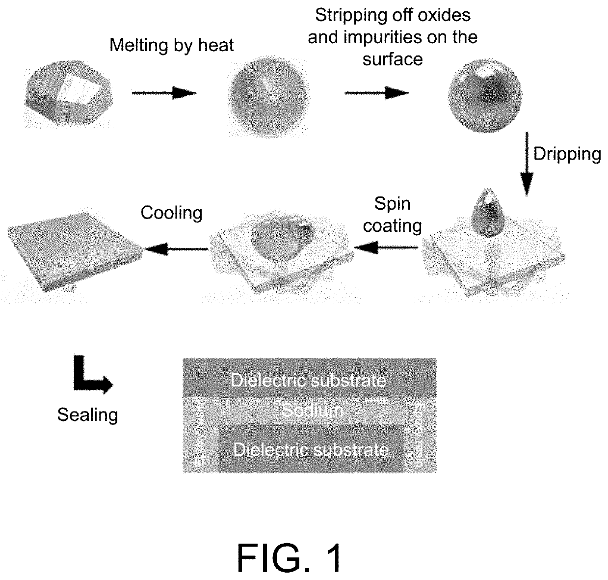
[0035]1. a sodium block with a certain size was placed in a tungsten boat, oxides on the surface were cut off to enable the sodium block to have metallic luster, then the tungsten boat containing the sodium block was heated to 160° C. on a heating table to melt the sodium block into liquid, and oxides and impurities on the surface of the molten sodium were stripped off using stainless steel tweezers to form a liquid sodium pellet with metallic luster;

[0036]2. a smooth quartz substrate with a size of 1.5 cm×1.5 cm×0.2 mm was put into a glove box, and quickly spun on a spin coater; the quartz substrate with periodic structures was spin-coated with the pure liquid sodium metal by thermally-assisted spin coating at 16...

example 2

[0039

[0040]A sodium interface was prepared according to the method of Example 1, and the difference between these two methods is that, in the method of Example 2, a sodium block was melted at 180° C. by heat in step (1), and a quartz substrate was spin-coated with the resulting liquid sodium at 180° C. and 8000 r / min in step (2). The prepared sodium interface was close to that of Example 1, and both had a smooth and flat surface.

example 3

[0041

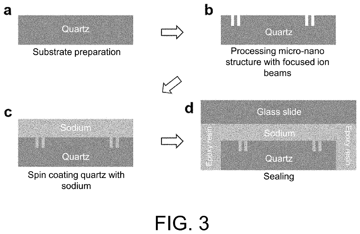
[0042]A sodium-based micro-nano optical structure device was prepared as in FIG. 3 by the following specific steps.

[0043](1) a micro-nano structure was processed on a dielectric substrate:

[0044]A. a silver film with a thickness of about 30 nm was subjected to physical vapor deposition on a quartz substrate with a size of 1.5 cm×1.5 cm×0.2 mm to form a conductive layer;

[0045]B. a periodic pore array with a pore size of 300 nm, a period of 700 nm and a depth of 55 nm was etched on the quartz substrate coated with silver using a focused ion beam, wherein the array had a length of 1.4 μm and a width of 0.7 μm, and a pore array with the same period size was processed at an interval of 100 μm, such that the distance between these two periodic arrays was 100 μm;

[0046]C. the silver on the surface of the quartz substrate was removed with nitric acid to obtain the quartz substrate only having the periodic pore arrays, as shown in b of FIG. 3. The quartz plate was ultrasonically cleaned f...


PUM

PropertyMeasurementUnit
Temperatureaaaaaaaaaa
Fractionaaaaaaaaaa
Concentrationaaaaaaaaaa

Abstract

The present invention discloses a method for preparing a sodium interface and a method for preparing a sodium-based optical structure device. This sodium interface is prepared in an inert gas atmosphere by the following steps: (1) melting solid sodium metal into liquid by heat, and stripping off solid oxides and impurities on the surface of the molten sodium metal to obtain pure liquid sodium with metallic luster; and (2) spin-coating a dielectric substrate with the liquid sodium to obtain the sodium interface tightly attached to the dielectric substrate. The prepared sodium interface can be used as a plasmon polariton material for use in plasmon polariton optical waveguides, nano-lasers and the like.

Description

TECHNICAL FIELD[0001]The present invention relates to the preparation of an alkali metal sodium interface, in particular to a method for preparing a sodium interface and a method for preparing a sodium-based optical structure device based on this method, and belongs to the technical field of metal surface plasmon polariton materials.DESCRIPTION OF RELATED ART[0002]Metal surface plasmon polariton materials have been widely concerned due to their wide application in integrated photovoltaics, photodetection, nano-lasers and other fields. Among plasmon polariton materials, noble metals such as gold and silver are the two most commonly used materials because of their relatively low losses in the visible and near-infrared bands. However, these two metals suffer great optical losses in plasmon polariton application, limiting the performance of devices. Besides, as noble metals, they are costly. Therefore, a material featuring a lower loss and lower cost is required. Alkali metal sodium was...

Claims


Application Information

Patent Timeline
IPC IPC(8): C23C26/02G02B5/08G02B1/10B05D1/00
CPCC23C26/02B05D1/005G02B1/10G02B5/0808G02B1/005
Inventor ZHU, JIAYU, JIANYUWANG, YANG
Owner NANJING UNIV
Why Eureka
Try Eureka