
Method of detecting defect and system of detecting defect

Pending Publication Date: 2022-03-03
SAMSUNG DISPLAY CO LTD
View PDF0 Cites 0 Cited by
  • Summary
  • Abstract
  • Description
  • Claims
  • Application Information

AI Technical Summary

Benefits of technology

The patent text describes a method and system for detecting defects in a stacked structure of a display panel using deep learning. This system can automatically determine the location of the defect and prevent data loss. It also utilizes a database for statistical analysis of image data, which helps identify process abnormalities and improve production efficiency. Overall, the technology helps reduce human and cost loss while improving the quality of the finished display panel.

Problems solved by technology

A determination of a location of a defect may be performed by engineers, so that data information may be lost and a determination time may increase.
In addition, a conventional object detection technology using an artificial intelligence deep learning has a limitation in that it only checks a type of an object and a simple location information in a single image.

Method used


Image

  • Method of detecting defect and system of detecting defect
  • Method of detecting defect and system of detecting defect
  • Method of detecting defect and system of detecting defect

Examples


Embodiment Construction

[0033]Hereinafter, embodiments will be described in detail with reference to the accompanying drawings so that those of ordinary skill in the art may easily implement the invention. However, the invention may be implemented in various different forms, and is not limited to the embodiments described herein. In the drawings, parts irrelevant to the description are omitted in order to clearly describe the invention, and similar reference numerals are assigned to similar parts throughout the specification.

[0034]It will be understood that when an element is referred to as being “on” another element, it can be directly on the other element or intervening elements may be therebetween. In contrast, when an element is referred to as being “directly on” another element, there are no intervening elements present.

[0035]It will be understood that, although the terms “first,”“second,”“third” etc. may be used herein to describe various elements, components, regions, layers and / or sections, these e...


PUM


Abstract

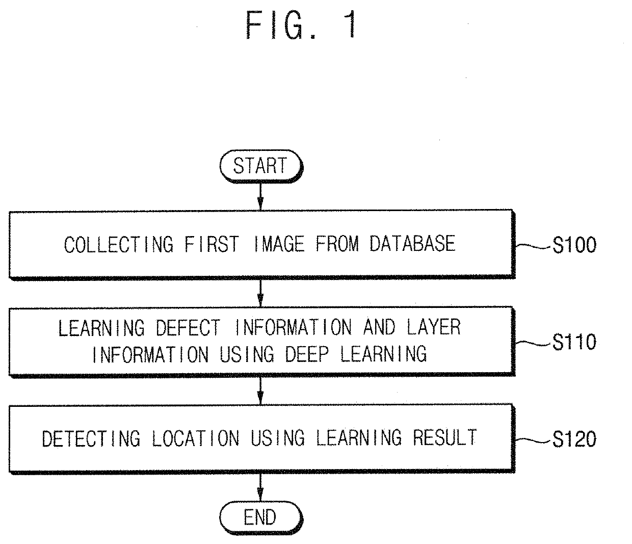
A method of detecting a defect in a stacked structure of a display panel includes collecting a first image of the defect and a plurality of layers in the stacked structure from a database, learning a defect information of the defect and a layer information of the layers using a deep learning model based on the first image and detecting a location of the defect among the layers by the defect information and the layer information.

Description

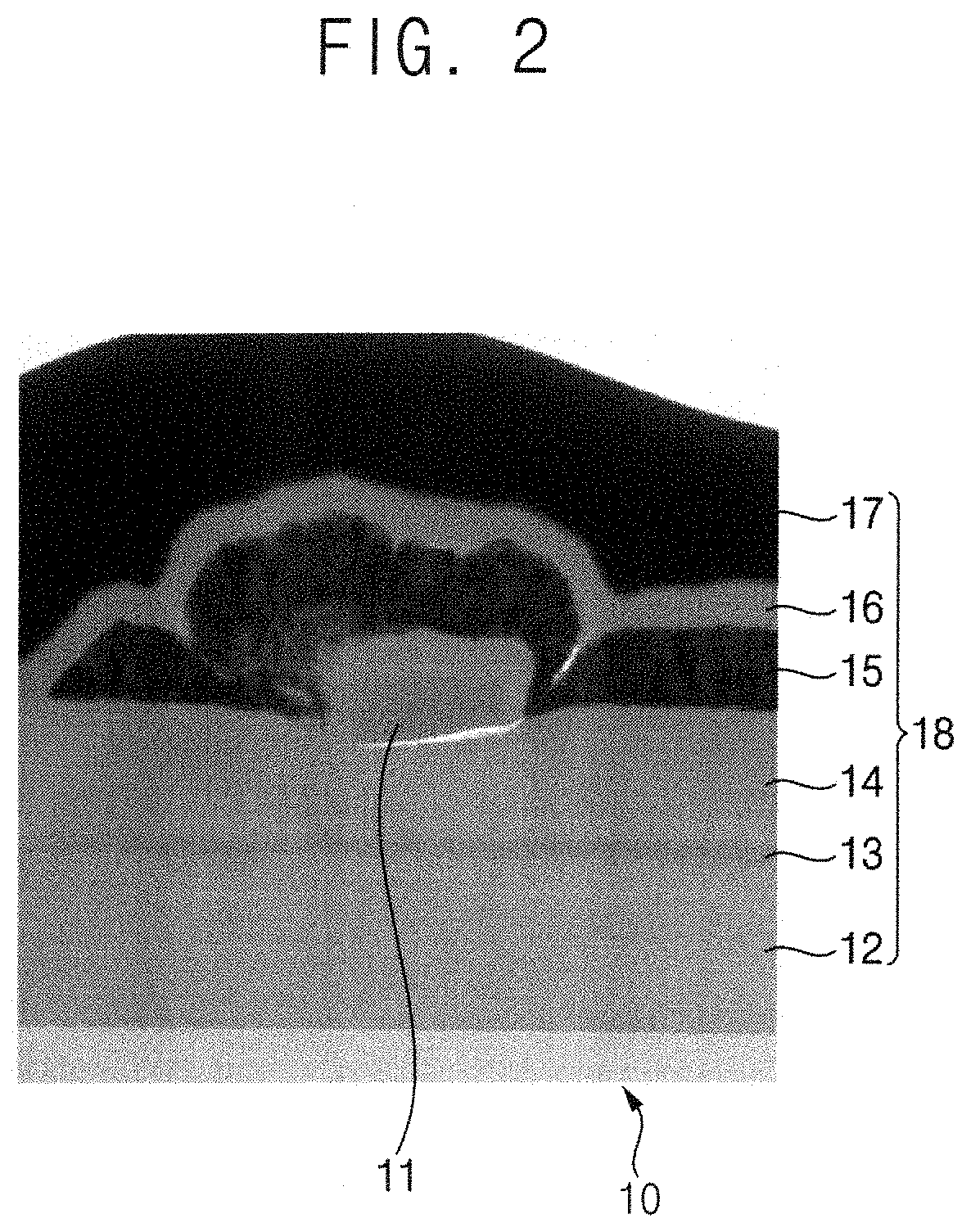
[0001]This application claims priority to Korean Patent Application No. 10-2020-0108417 filed on Aug. 27, 2020, and all the benefits accruing therefrom under 35 U.S.C. § 119, the content of which in its entirety is herein incorporated by reference.BACKGROUND1. Field[0002]Embodiments relate to a method of detecting a defect. More particularly, embodiments relate to a method and a system of detecting a defect in which a transmission electron microscope (“TEM”) image, a scanning electron microscope (“SEM”) image, a scanning transmission electron microscope (“STEM”) image, a secondary ion microscope (“SIM”) image and an energy dispersive X-ray spectroscopy (“EDS”) elemental mapping image may be learned using a deep learning and then detailed location information of the defect may be detected by combining them.2. Description of the Related Art[0003]It is possible to detect which layer of a stacked structure of a display panel has a defect using a transmission electron microscope (“TEM”) ...

Claims


Application Information

Patent Timeline
IPC IPC(8): G06T7/00G06T7/70G06N3/04G06N3/08
CPCG06T7/0004G06T7/70G06N3/04G06T2207/20084G06T2207/20081G06T2207/10061G06T2207/10116G06N3/08G06N3/045G01N21/8851G01N23/2251G01N23/2257G01N21/95G01N2021/8887G01N2021/9513
Inventor PARK, YOUNGGILKIM, KIHYUNLEE, YOUNGUOOK
Owner SAMSUNG DISPLAY CO LTD
Learn More