A method for detecting defects in thin film layers

Pending Publication Date: 2021-11-04
MEMSSTAR
View PDF4 Cites 0 Cited by
  • Summary
  • Abstract
  • Description
  • Claims
  • Application Information

AI Technical Summary

Benefits of technology

The patent is about a method for improving the detection of defects in a thin film layer. By exposing the layer to a vapor phase etchant, the method can enhance any defects present in the layer. By analyzing and comparing multiple images of the layer, the method can increase accuracy in identifying defects by minimizing measurement uncertainty. The test chamber used for the method includes a pressure gauge to control the pressure and vapor etchant density. The technical effect of this patent is improved detection and identification of defects in thin film layers.

Problems solved by technology

Should a pinhole exist in a given structure this can lead to a failure.
In the example of a flat panel screen for use within a television, should a pinhole defect be discovered, this can lead to a failed end product with dead image regions which show up as black dots on the screen when an image is shown.
Similarly, in solar cells, early identification of defects allows for cells with a high likelihood of failure to be removed from further production steps and, as a result, minimise wasted costs.
These failures would cause a significant drop in energy conversion from solar to electrical due to the failed regions not absorbing sunlight.
In the case of electrical devices, due to the nature of manufacture in which multiple devices could be manufactured in a single process run, identification of defects again allows for electrical devices with a high likelihood of failure to be removed from final manufacturing stages and sending out failed devices.
These failure methods are numerous and varied, but their presence can cause significant levels of lost revenue.
The primary issue with pinholes is that the required minimum detectable pinhole size is continually decreasing yet the current detection methods are beginning to encounter limits.
A major issue with the current detection methods is the global exposure to this etching solution, typically in an acid form, which may result in damage to otherwise viable devices elsewhere on the same test sample.
In practice, the minimum detectable pinhole size is limited by the wet etchant mobility and this minimum detectable pinhole size may not be sufficient for detecting all potential failure inducing defects in a thin film layer.
Furthermore, as electronic devices continue to shrink in dimension, the pinhole defects capable of resulting in a device failure are also become smaller whilst increasing tolerances are required in the manufacture of the electronic devices.
This also means that each type of product or device has its own “critical pinhole” threshold which is considered large enough to result in a high likelihood of failure.
Existing wet etching processes utilised in defect detection do not allow for customisation or control of the process.
Furthermore, due to the destructive nature of existing wet etching processes the test sample can only be tested using one method.

Method used


Image

  • A method for detecting defects in thin film layers
  • A method for detecting defects in thin film layers
  • A method for detecting defects in thin film layers

Examples


Embodiment Construction

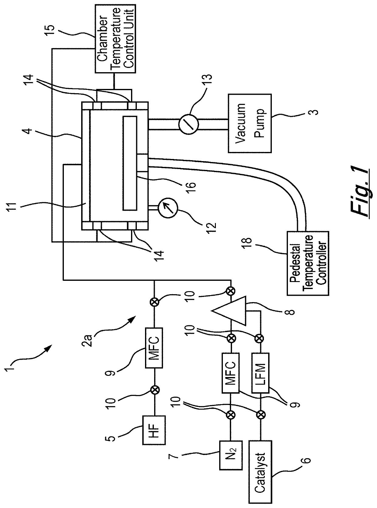
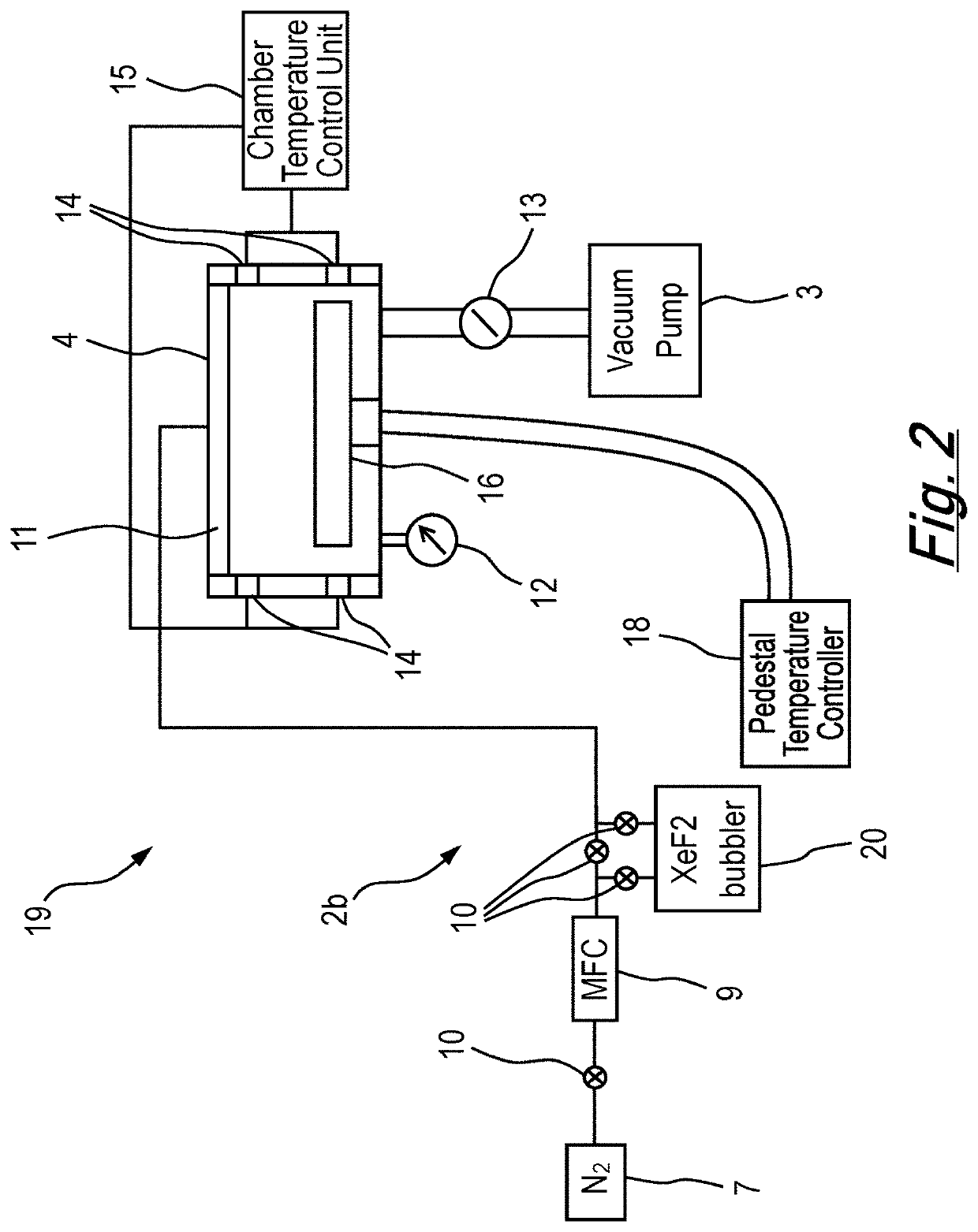
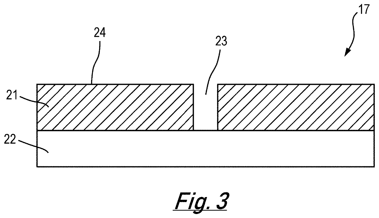
[0060]An explanation of the present invention will now be described with reference to FIGS. 1 to 7.

[0061]According to a first embodiment, FIG. 1 depicts a hydrogen fluoride (HF) vapour-based testing system 1 comprising a gas delivery system 2a and a vacuum pump 3 in fluid communication via a test chamber 4.

[0062]The gas delivery system 2a comprises an HF vapour source 5, a catalyst source 6 which takes the form of a water or alcohol source, a nitrogen gas source 7 and a vaporiser 8. Catalyst vapour for use within the test chamber 4 is produced by connecting the catalyst source 6 to the vaporiser 8. The nitrogen gas source 7 is a standard element of the vaporiser 8, and acts as a carrier gas to assist in transporting the catalyst vapour to the test chamber 4. When utilised, the catalyst vapour is employed during the HF vapour etch. Mass Flow Controllers or Liquid Flow Meters (MFC / LFM) 9 and pneumatic valves 10 are preferably provided within each supply line of the gas delivery system...


PUM


Abstract

A method of detecting defects in a structure sample comprising a thin film layer and a sacrificial later is disclosed. The method comprises exposing the thin film layer to a vapour phase etchant, obtaining an image of the thin film layer and analysing the image. The vapour phase etchant enhances any defects present in the thin film layer by passing through the defect and etching a cavity within the sacrificial layer. The cavity undercuts the thin film layer resulting in a stress region surrounding the defect. Defects which were not originally detectable may be made detectable after exposure to the vapour phase etchant. A vapour phase etchant has the advantage of being highly mobile such that it can access defects that a liquid phase etchant might not. Furthermore, unlike a liquid phase etchant, a vapour phase etchant can be used to test a sample non-destructively.

Description

[0001]The present invention relates to the field of thin film layer processing. More specifically, the present invention concerns the detection of defects in thin film layers.BACKGROUND TO THE INVENTION[0002]A thin film layer is deposited on to a substrate layer to form a structure. A structure may comprise multiple layers. A layer may, by itself or in conjunction with other layers, be functional. For example, a layer may be conductive or have a desired mechanical property. Such a structure may function as or form part of an electrical device, a solar cell, a flat panel screen for a television or a photo mask, for example. In order to produce a reliable structure, a method of determining whether the thin film layer is defect free is preferred as a means to identify failures in the structure. An example of a defect in a thin film layer is a pinhole. Pinholes cannot be viewed by the human eye or even a microscope, but it is possible to enhance their visibility with the help of additio...

Claims


Application Information

Patent Timeline
IPC IPC(8): G01N21/84G01N21/88
CPCG01N21/8422H01L21/32135G01N2021/8438G01N21/8851H01L22/24G01N21/9501G01N2021/8427G01N21/8803G01N21/91G01N2021/9513H01L21/30621G06T7/0004G01N2021/8887
Inventor O'HARA, ANTHONYDRYSDALE, DANIEL
Owner MEMSSTAR
Why Eureka
Try Eureka