Display panel

Active Publication Date: 2021-02-18
SHENZHEN CHINA STAR OPTOELECTRONICS SEMICON DISPLAY TECH CO LTD
View PDF0 Cites 0 Cited by
  • Summary
  • Abstract
  • Description
  • Claims
  • Application Information

AI Technical Summary

Benefits of technology

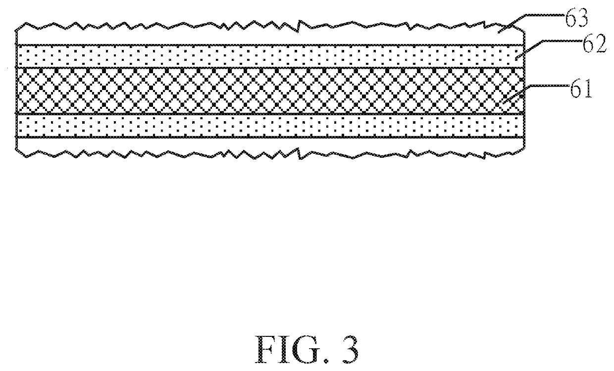
The present invention provides a display panel that solves the issue of abnormal display due to anode oxidization. The panel includes a substrate, a thin film transistor layer, and a light emitting diode structure. The light emitting diode structure includes an anode, a light emitting material layer, and a cathode. An anode reflective layer is located under the anode and is insulated from the anode through a reflective insulation layer. A quantum dot thin film is located between the anode and the anode reflective layer. The anode reflective layer can be made of silver, copper, aluminum, or a combination of these materials. The quantum dot thin film includes a quantum dot material layer, a barrier layer, and a protective layer. The quantum dots in the quantum dot thin film emit light of different colors, and the size of the quantum dots corresponds to the color of light emitted. The quantum dot material layer includes high molecular polymer and quantum dots evenly distributed in the high molecular polymer. The quantum dots can be silicon quantum dots, germanium quantum dots, cadmium sulfide quantum dots, or a combination of these quantum dots. The present invention improves light emitting efficiency and use rate of light, reduces pixel failure due to oxidization of the reflective material, and simplifies the process of disposing the quantum dot thin film.

Problems solved by technology

However, Ag easily oxidizes in the air to form oxidized silver bumps, which results in that shorting of the anode and the cathode of OLED device to cause pixels to be unable to emit light and thus influences quality of displayed images.

Method used


Image

  • Display panel
  • Display panel
  • Display panel

Examples


Embodiment Construction

[0034]Each of the following embodiments is described with appending figures to illustrate specific embodiments of the present invention that are applicable. The terminologies of direction mentioned in the present invention, such as “upper”, “lower”, “front”, “rear”, “left”, “right”, “inner”, “outer”, “side surface”, etc., only refer to the directions of the appended figures. Therefore, the terminologies of direction are used for explanation and comprehension of the present invention, instead of limiting the present invention. In the figures, units with similar structures are marked with the same reference characters.

[0035]With reference to FIG. 1, FIG. 1 is a schematic structural view of a conventional display panel. The display panel is a top emission display panel. In other words, a light output surface of the display panel is a surface of a cathode of a light emitting diode structure away from an anode.

[0036]With reference to FIG. 1, the conventional display panel comprises a sub...


PUM


Abstract

The present invention provides a display panel including a light emitting diode structure. The light emitting diode structure includes an anode located on a thin film transistor layer, a light emitting material layer located on the anode, and a cathode covering the light emitting material layer. The light emitting diode structure further includes an anode reflective layer and a quantum dot thin film. The anode reflective layer is located under the anode, and is electrically insulated from the anode through a reflective insulation layer. The quantum dot thin film is located between the anode and the anode reflective layer.

Description

FIELD OF INVENTION[0001]The present invention relates to a field of electronic displays, especially to a display panel.BACKGROUND OF INVENTION[0002]Organic light emitting diode (OLED) display panels have characteristics of self-luminescence, high brightness, wide view angle, high contrast, flexibility, and low energy consumption, and are therefore applied extensively to mobile phone screens, displays, monitors, and color televisions.[0003]Technical Issue[0004]An anode of a top emission organic light emitting diode (OLED) structure generally employs a structure constructed by indium tin oxide (ITO) and silver (Ag). To match energy levels of the anode and the organic light emitting material, a material of the anode directly contacting the organic material is the ITO. Furthermore, because the anode needs to serve as a reflective electrode, the anode needs to be disposed with metal with a high reflectivity, for example, Ag.[0005]However, Ag easily oxidizes in the air to form oxidized si...

Claims


Application Information

Patent Timeline
IPC IPC(8): H01L51/52H01L27/32
CPCH01L51/5253H01L27/3248H01L51/5218H01L2251/5369H01L27/3246H01L51/5271H01L27/322H10K50/818H10K2102/103H10K2102/331H10K2102/3026H10K50/844H10K50/856H10K59/38H10K59/122H10K59/123
Inventor ZENG, WEIJING
Owner SHENZHEN CHINA STAR OPTOELECTRONICS SEMICON DISPLAY TECH CO LTD
Why Eureka
Try Eureka