Nitride semiconductor light emitting element and method for manufacturing the same

Inactive Publication Date: 2016-06-09
USHIO DENKI KK
View PDF4 Cites 2 Cited by
  • Summary
  • Abstract
  • Description
  • Claims
  • Application Information

AI Technical Summary

Benefits of technology

The present invention provides a nitride semiconductor light-emitting element that has excellent lifespan characteristics and is more efficient in light emission compared to conventional elements.

Problems solved by technology

Conversely, when the well layer is doped with impurities, the crystallinity is deteriorated, so that the scattering of carriers increases, whereby the threshold tends to increase.

Method used


Image

  • Nitride semiconductor light emitting element and method for manufacturing the same
  • Nitride semiconductor light emitting element and method for manufacturing the same
  • Nitride semiconductor light emitting element and method for manufacturing the same

Examples


example 1

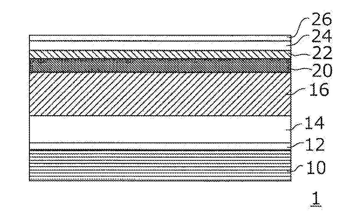
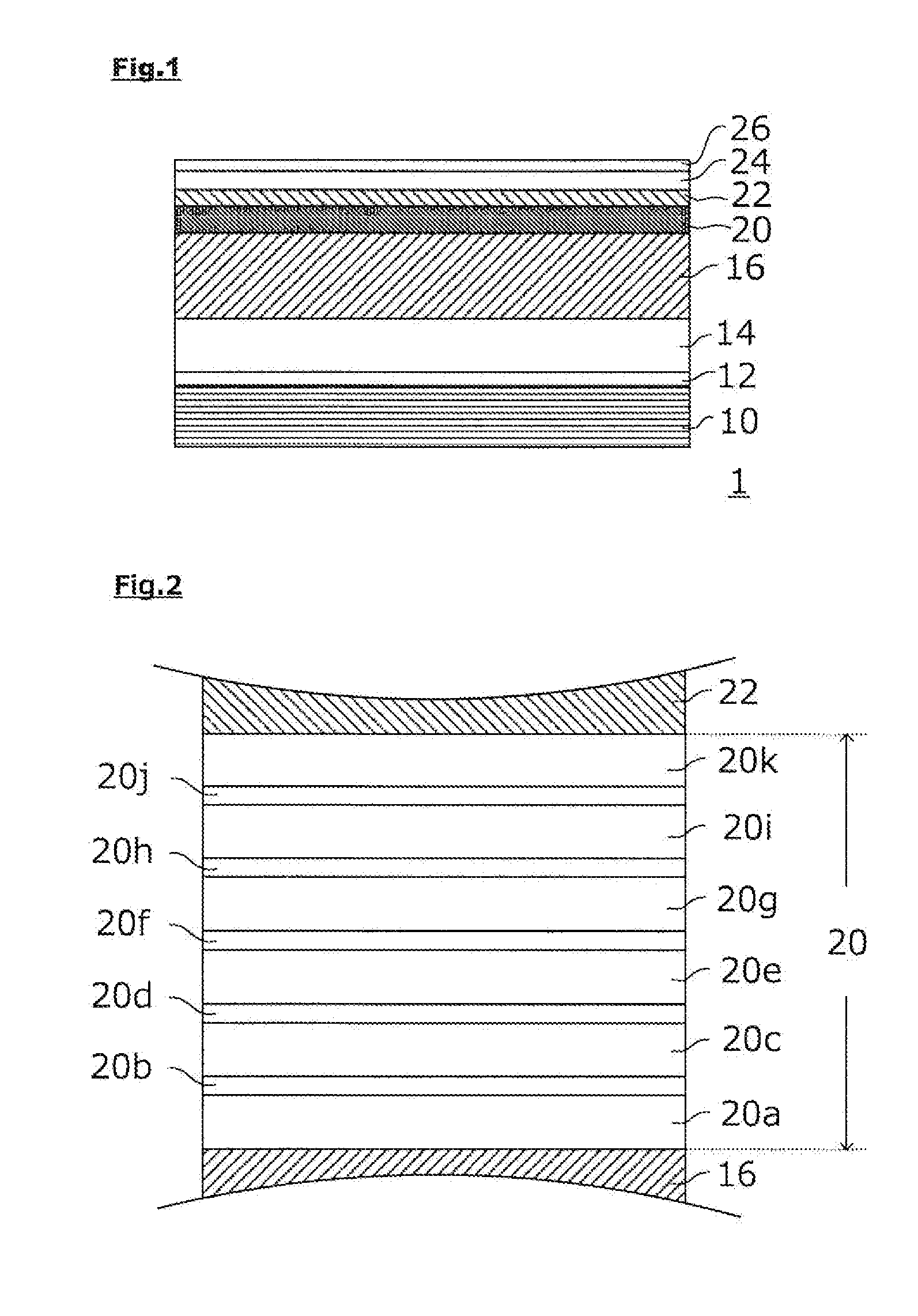
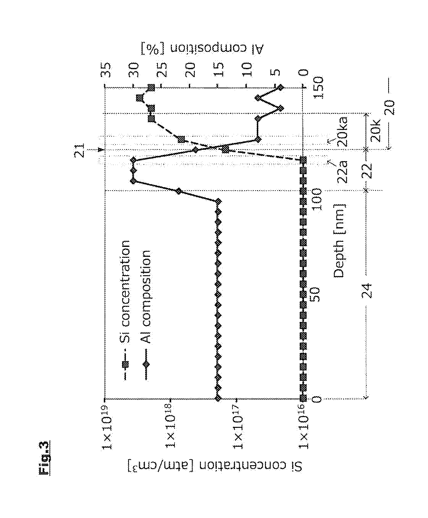
[0053]All the barrier layers were set to have a thickness of 20 nm, and these were allowed to contain n-type impurities. Further, the final barrier layer 20k was formed so that the n-type impurity concentration at the interface with the p-type nitride semiconductor layer 22 would be 3×10¹⁶ / cm3.

[0054]In forming the final barrier layer 20k, tetraethylsilane (TESi), which is a source material gas for doping with Si constituting the n-type impurity, is mixed in addition to nitrogen, hydrogen, trimethylgallium (TMG), and trimethylaluminum (TMA) that constitute a source material gas of AlbGa1-bN, and the final barrier layer 20k is grown for a predetermined period of time. Thereafter, only the supply of TESi is stopped, and the growth is continued. This allows that the Si with which the final barrier layer 20k is doped by supply of TESi, that is, the n-type impurity, is diffused to the surface side of the final barrier layer 20k. By controlling the period of time for supplying TESi, the n-...

example 2

[0066]An element was formed in the same manner as in Example 1 except that, in forming the final barrier layer 20k, the period of time for supplying TESi was set to be about 240 seconds to grow the final barrier layer 20k to 10 nm while allowing the final barrier layer 20k to contain the n-type impurity and that, by stopping the supply of TESi thereafter and supplying nitrogen, hydrogen, TMG, and TMA for about 240 seconds, the final barrier layer 20k eventually having a thickness of 20 nm was formed in about 480 seconds. This allowed that, in the element of Example 2, the n-type impurity concentration at the interface between the final barrier layer 20k and the p-type nitride semiconductor layer 22 was 7×10¹⁶ / cm3.

example 3

[0067]An element was formed under the same conditions as in Example 2 except that a part of the barrier layers (20a, 20c, 20e, 20g, 20i, 20k), that is, the barrier layer 20g, was left undoped.


PUM

PropertyMeasurementUnit
Efficiencyaaaaaaaaaa
Semiconductor propertiesaaaaaaaaaa

Abstract

To realize a nitride semiconductor light-emitting element having excellent lifespan characteristics in addition to improved light emission efficiency compared with conventional elements. A nitride semiconductor light-emitting element having a light-emitting layer obtained by alternately stacking a well layer comprising a nitride semiconductor and a barrier layer comprising a nitride semiconductor between an n-type nitride semiconductor layer and a p-type nitride semiconductor layer, wherein a final barrier layer, which is the barrier layer formed at a position in contact with the p-type nitride semiconductor layer, contains n-type impurities, and the concentration of n-type impurities at the interface with the p-type nitride semiconductor layer is 4×10¹⁷ / cm3 or less.

Description

TECHNICAL FIELD[0001]The present invention relates to a nitride semiconductor light-emitting element having a light-emitting layer obtained by alternately stacking at least one well layer including a nitride semiconductor and at least one barrier layer including a nitride semiconductor between an n-type nitride semiconductor layer and a p-type nitride semiconductor layer, as well as to a method for manufacturing the same.BACKGROUND ART[0002]Today, a nitride semiconductor is used and developed for use in various light-emitting elements such as an LED (light-emitting diode) and an LD (laser diode) (for example, see Patent Documents 1 and 2). Recently, the nitride semiconductor is being developed also for use in an element that emits ultraviolet light or light having a shorter wavelength than that.[0003]Generally, in a nitride semiconductor light-emitting element, a structure is adopted in which a light-emitting layer obtained by alternately stacking at least one well layer including a...

Claims


Application Information

Patent Timeline
IPC IPC(8): H01L33/32H01L33/00
CPCH01L33/0075H01L33/325H01L33/32H01L33/025H01L33/06H01L33/12C23C16/52C23C16/0227C23C16/0209H01L33/007C23C16/303
Inventor TSUKIHARA, MASSASHIMIYOSHI, KOHEI
Owner USHIO DENKI KK
Why Eureka
Try Eureka