Display apparatus
- Summary
- Abstract
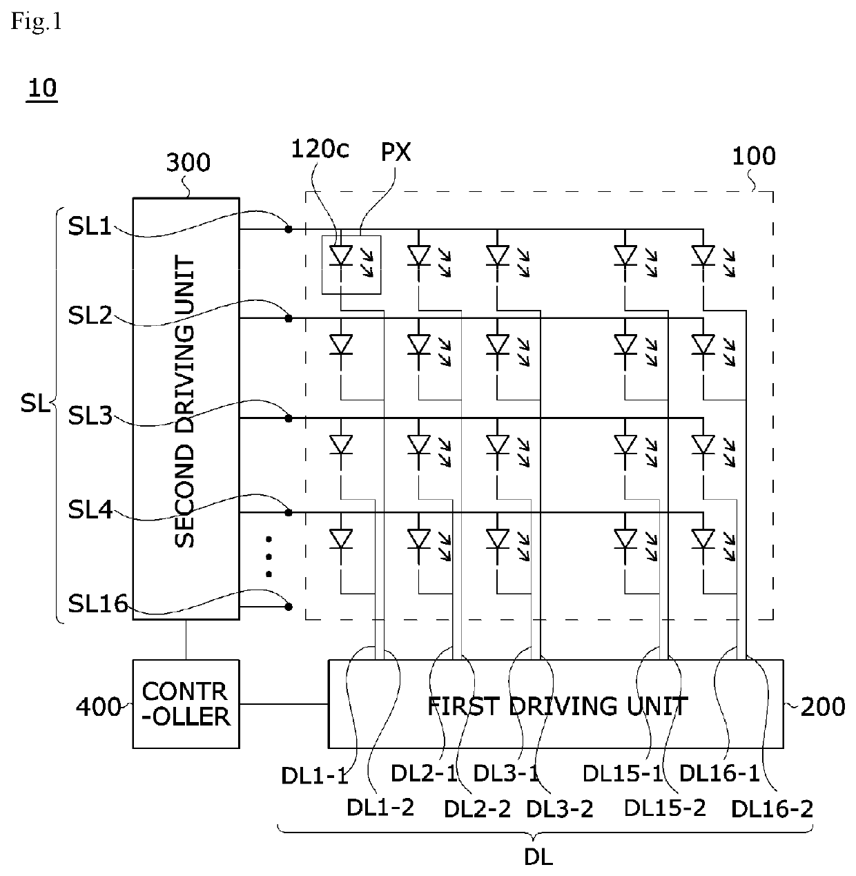
- Description
- Claims
- Application Information
AI Technical Summary
Benefits of technology
Problems solved by technology
Method used
Image

Examples
Embodiment Construction
[0096]While the present invention is open to various modifications and alternative embodiments, specific embodiments thereof will be described and shown by way of example in the accompanying drawings. However, it should be understood that there is no intention to limit the present invention to the particular embodiments disclosed, and, on the contrary, the present invention is to cover all modifications, equivalents, and alternatives falling within the spirit and scope of the present invention.
[0097]It should be understood that, although the terms including ordinal numbers such as first, second, and the like may be used herein to describe various elements, the elements are not limited by the terms. The terms are used only for the purpose of distinguishing one element from another. For example, without departing from the scope of the present invention, a second element could be termed a first element, and similarly a first element could be also termed a second element. The term “and / ...
PUM
 Abstract
Description
Claims
Application Information
 - R&D
- Intellectual Property
- Life Sciences
- Materials
- Tech Scout
- Unparalleled Data Quality
- Higher Quality Content
- 60% Fewer Hallucinations
Browse by: Latest US Patents, China's latest patents, Technical Efficacy Thesaurus, Application Domain, Technology Topic, Popular Technical Reports.
© 2025 PatSnap. All rights reserved.Legal|Privacy policy|Modern Slavery Act Transparency Statement|Sitemap|About US| Contact US: help@patsnap.com