High-frequency front-end circuit
- Summary
- Abstract
- Description
- Claims
- Application Information
AI Technical Summary
Benefits of technology
Problems solved by technology
Method used
Image

Examples
first embodiment
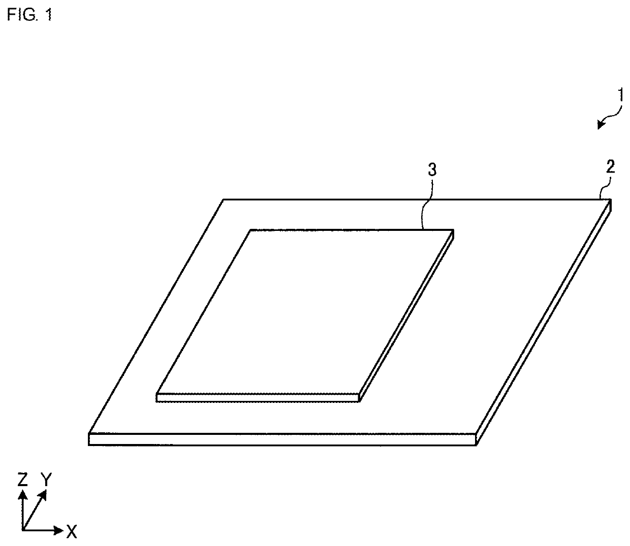
[0020]FIG. 1 illustrates an external appearance of a high-frequency front-end circuit according to a first embodiment. A high-frequency front-end circuit 1 according to the first embodiment includes a substrate 2 and a substrate 3.
[0021]The high-frequency front-end circuit 1 can be used in a mobile wireless communication terminal device, such as a cellular phone or a smartphone, to transmit and receive various signals of, for example, voice and data, to and from a base station.
[0022]The substrate 2 is a non-semiconductor substrate. Examples of the substrate 2 may include a rigid substrate made of, for example, a glass epoxy resin or low-temperature co-fired ceramic (LTCC) and a flexible substrate made of, for example, a liquid crystal polymer or polyimide resin.
[0023]The substrate 3 is a semiconductor substrate. As the substrate 3, an integrated circuit (IC) chip (die) is illustrated as an example.
[0024]The substrate 2 is substantially parallel with an X-Y plane. The substrate 3 is ...
second embodiment
[0046]FIG. 5 is a schematic diagram illustrating a configuration of a high-frequency front-end circuit according to a second embodiment. The same elements as those in the first embodiment have the same reference numerals and are not described here.
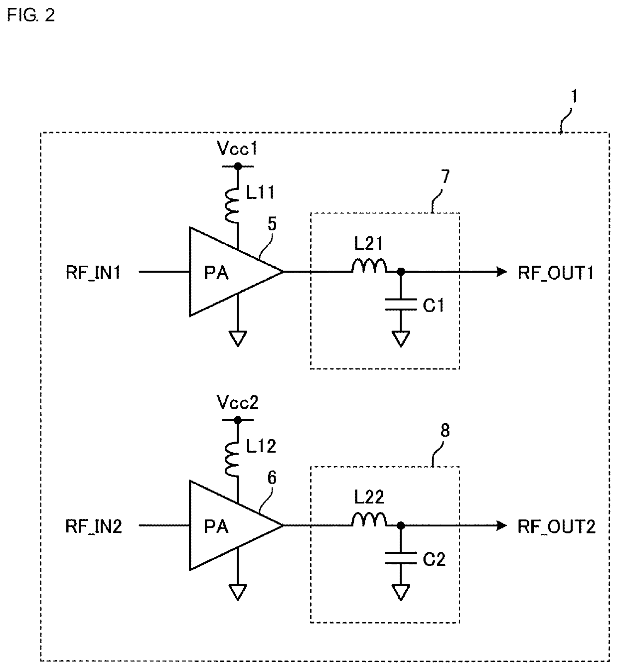
[0047]In the present embodiment, the first power amplifier 5, second power amplifier 6, first power supply inductor L11, second power supply inductor L12, first matching inductor L21, and second matching inductor L22 are disposed on or in a substrate 3a.
[0048]In the present embodiment, the substrate 3a is a semiconductor substrate and constitutes an IC chip arranged on the substrate 2. The IC chip includes the first power amplifier 5, second power amplifier 6, first power supply inductor L11, second power supply inductor L12, first matching inductor L21, and second matching inductor L22, and is mounted on the substrate 2, which is a non-semiconductor substrate, and they constitute a high-frequency front-end circuit 1a. In the present embo...
third embodiment
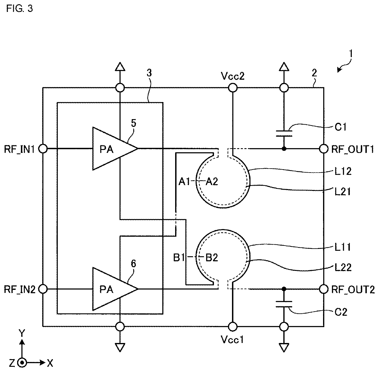
[0053]FIG. 6 illustrates an external appearance of a high-frequency front-end circuit according to a third embodiment. FIG. 7 is a schematic diagram illustrating a configuration of the high-frequency front-end circuit according to the third embodiment. The same elements as those in the first and second embodiments have the same reference numerals and are not described here.
[0054]A high-frequency front-end circuit 1b according to the third embodiment includes the substrate 2, the substrate 3, and a substrate 4.
[0055]The substrate 4 is a semiconductor substrate. As the substrate 4, an integrated passive device (IPD) is illustrated as an example.
[0056]The substrate 4 is substantially parallel with an X-Y plane. As viewed from a Z direction, the substrate 4 overlaps the substrate 2. The substrate 2 has an area equal to or larger than the region overlapping the substrates 3 and 4.
[0057]In the present embodiment, the first power amplifier 5 and second power amplifier 6 are disposed on the...
PUM
 Abstract
Description
Claims
Application Information
 - R&D
- Intellectual Property
- Life Sciences
- Materials
- Tech Scout
- Unparalleled Data Quality
- Higher Quality Content
- 60% Fewer Hallucinations
Browse by: Latest US Patents, China's latest patents, Technical Efficacy Thesaurus, Application Domain, Technology Topic, Popular Technical Reports.
© 2025 PatSnap. All rights reserved.Legal|Privacy policy|Modern Slavery Act Transparency Statement|Sitemap|About US| Contact US: help@patsnap.com