Wire bonding apparatus and manufacturing method for semiconductor apparatus

Active Publication Date: 2020-06-25
SHINKAWA CO LTD
View PDF0 Cites 0 Cited by
  • Summary
  • Abstract
  • Description
  • Claims
  • Application Information

AI Technical Summary

Benefits of technology

The present invention is aimed at providing a wire bonding apparatus and manufacturing method for semiconductor devices that can perform good wire bonding while satisfying the demand for maintainability and size reduction. The wire bonding apparatus includes a bonding arm, an ultrasonic horn, a bonding tool, a first tensioner, a second tensioner, and a control part. The control part implements control to turn off or make smaller the second gas flow of the second tensioner after the first bonding step. The technical effect of the invention is that it allows for a suitable loop to be formed without reducing the bonding processing speed, and a separate clamper for making wire tension is not required.

Problems solved by technology

In this case, for example, if the wire tension is too large during the formation of the wire loop, the wire may be excessively stretched and the loop shape may be broken.
Alternatively, if the wire tension is too large during bonding to the second bonding point, the wire may be cut off during the bonding, and wire falling in which the wire falls out of the bonding tool may occur.

Method used


Image

  • Wire bonding apparatus and manufacturing method for semiconductor apparatus
  • Wire bonding apparatus and manufacturing method for semiconductor apparatus
  • Wire bonding apparatus and manufacturing method for semiconductor apparatus

Examples


first embodiment

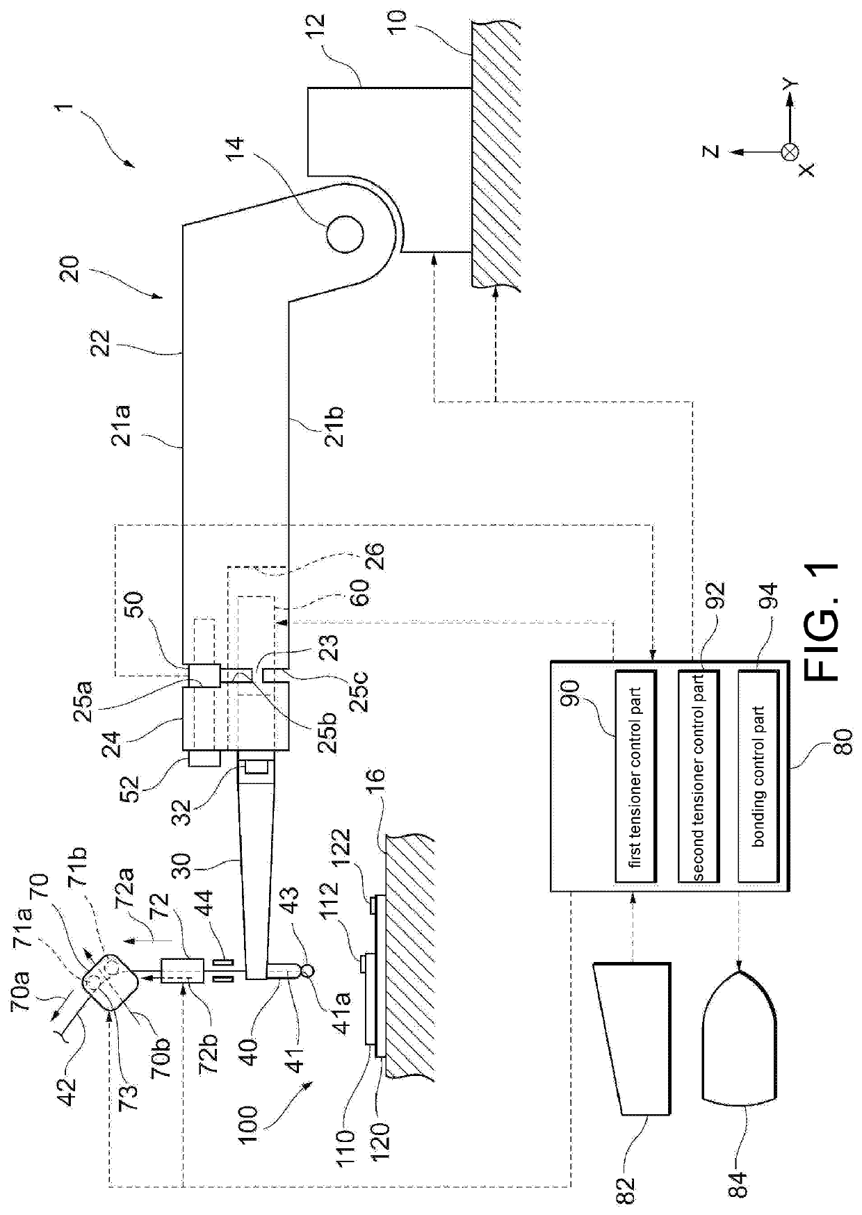
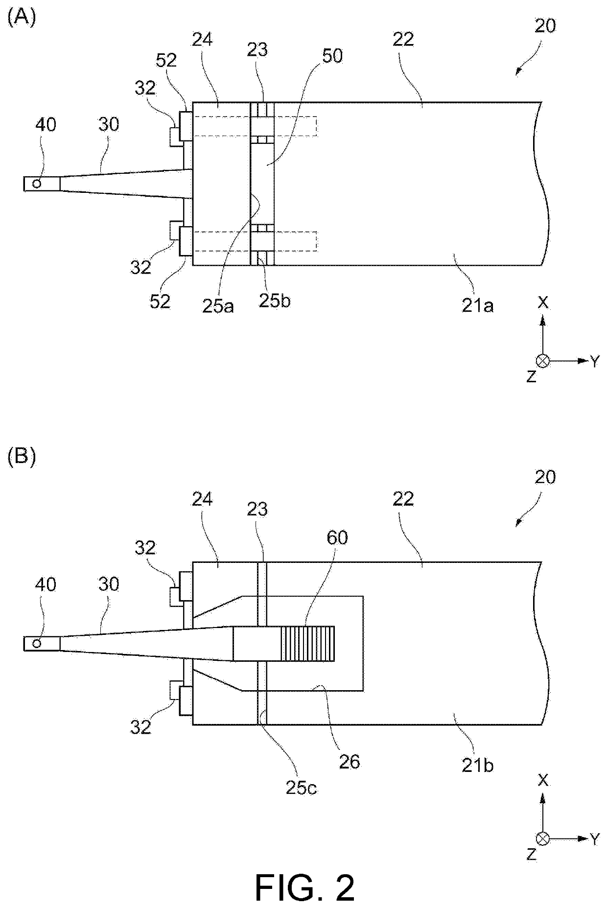
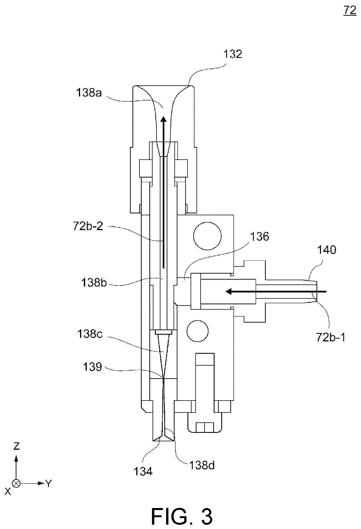
[0020]FIG. 1 is a diagram showing an overall outline of a wire bonding apparatus of the embodiment. In addition, FIGS. 2(A) and 2(B) are partially enlarged views of a bonding arm in the wire bonding apparatus. Specifically, FIG. 2(A) shows a top view of the bonding arm, and FIG. 2(B) shows a bottom view of the bonding arm. FIG. 3 is a diagram showing details of a second tensioner.

[0021]As shown in FIG. 1, a wire bonding apparatus 1 includes an XY drive mechanism 10, a Z drive mechanism 12, a bonding arm 20, an ultrasonic horn 30, a bonding tool 40, a load sensor 50, an ultrasonic vibrator 60, a first tensioner 70, a second tensioner 72, and a control part 80.

[0022]The XY drive mechanism 10 is configured to be slidable in an XY-axis direction (direction parallel to the bonding surface), and the Z drive mechanism (linear motor) 12 capable of swinging the bonding arm 20 in a Z-axis direction (direction perpendicular to the bonding surface) is arranged in the XY drive mechanism (linear ...

second embodiment

[0070]Next, a manufacturing method for semiconductor apparatus of a second embodiment of the present invention is described with reference to FIGS. 7(A)-7(G) and FIG. 8. FIGS. 7(A)-7(G) are schematic diagrams showing the operation, and FIG. 8 is a timing chart of FIGS. 7(A)-7(G). Besides, the times t4-t8 in FIGS. 7(A)-7(G) coincide with the times t4-t8 in FIG. 8. In the following embodiment, the same parts as those in the first embodiment are denoted by the same reference signs.

[0071]In the first embodiment, after the wire tail 42c connected to the wire loop 42a is formed, the wire tail 42d is formed by cutting off the wire 42 (FIGS. 5(F) and 5(D)). However, in the second embodiment, the wire tail 42c is formed at first after the wire 42 is cut off. In addition, in the second embodiment, the HIGH control is performed on both the first tensioner 70 and the second tensioner 72 in the period till time t5, and the OFF control is performed in the period from time t6a to time t7b. Hereina...

third embodiment

[0084]Next, a manufacturing method for semiconductor apparatus of a third embodiment of the present invention is described with reference to FIGS. 9(A)-9(F) and FIG. 10. FIGS. 9(A)-9(F) are schematic diagrams showing the operation, and FIG. 10 is a timing chart of FIGS. 9(A)-9(F). Besides, the times t4-t8 in FIGS. 9(A)-9(F) coincide with the times t4-t8 in FIG. 10. In the following embodiment, the same parts as those in the first embodiment are denoted by the same reference signs.

[0085]The third embodiment is the same as the first embodiment in terms of forming the wire tail 42d by cutting off the wire 42 after forming the wire tail 42c connected to the wire loop 42a. The third embodiment is different from the first embodiment in that the HIGH control is performed on both the first tensioner 70 and the second tensioner 72 in the period till time t4 and the OFF control is performed in the period from time t5 to time t6b. Hereinafter, points different from the first embodiment are des...


PUM


Abstract

A wire bonding apparatus includes: a first tensioner which forms, nearer a wire supply side than a bonding tool, a first gas flow for applying a tension toward the wire supply side on a wire; a second tensioner which forms, between the first tensioner and a pressing part of the bonding tool, a second gas flow for applying a tension toward the wire supply side on the wire; and a control part which controls the first tensioner and the second tensioner. The control part implements control, in a predetermined period after a first bonding step for bonding the wire to a first bonding point, to turn off at least the second gas flow of the second tensioner among the first tensioner and the second tensioner or to make at least the second gas flow smaller than in the first bonding step.

Description

BACKGROUND OF THE INVENTIONTechnical Field[0001]The present invention relates to a wire bonding apparatus and a manufacturing method for semiconductor apparatus.Related Art[0002]A wire bonding apparatus that electrically connects a first bonding point (for example, a pad of a semiconductor die) and a second bonding point (for example, a lead of a package) with a wire is known. In this wire bonding apparatus, it is general to apply a tension toward the wire supply side on the wire in a series of wire bonding operations for forming a wire loop that connects the first bonding point and the second bonding point.[0003]In this case, for example, if the wire tension is too large during the formation of the wire loop, the wire may be excessively stretched and the loop shape may be broken. Alternatively, if the wire tension is too large during bonding to the second bonding point, the wire may be cut off during the bonding, and wire falling in which the wire falls out of the bonding tool may ...

Claims


Application Information

Patent Timeline
IPC IPC(8): H01L23/00
CPCH01L2224/78353H01L24/85H01L2224/78631H01L24/43H01L24/78H01L2224/78821H01L21/67138H01L2224/48091H01L2224/48465H01L2224/78301H01L2224/78901H01L2924/00014H01L2224/85181H01L2224/85045H01L2224/85093H01L2224/77353H01L2224/859H01L24/48H01L2224/45099H01L2224/48227H01L2924/00H01L24/742H01L2224/78347H01L2224/78621H01L2224/78822H01L2225/1052
Inventor TEI, SHINSUKE
Owner SHINKAWA CO LTD
Why Eureka
Try Eureka