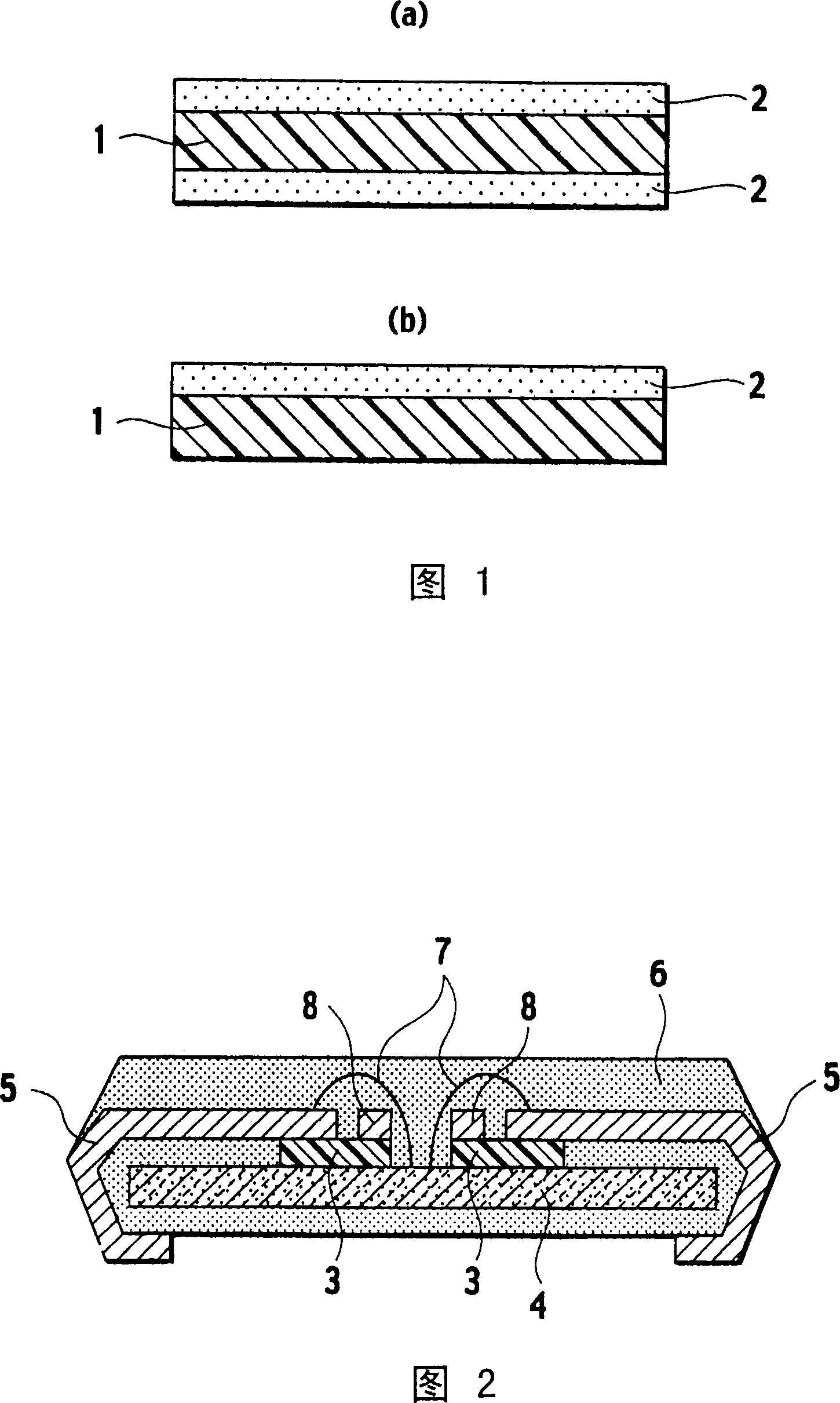
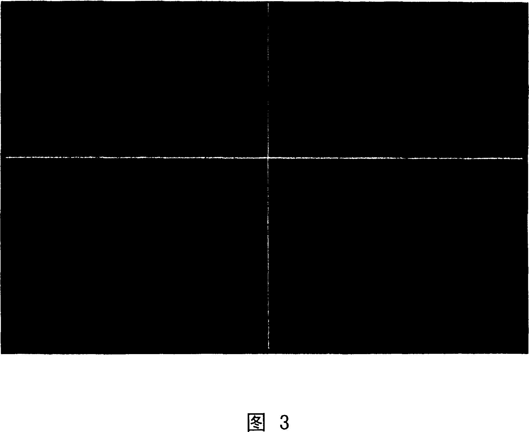
Adhesive film, lead frame with adhesive film, and semiconductor device using same
A technology for bonding films and lead frames, which is applied in semiconductor devices, semiconductor/solid-state device manufacturing, electric solid-state devices, etc. It can solve the problems of semiconductor chips and lead frames that cannot be electrically bonded, and achieve excellent bonding workability and compatibility Good, excellent adhesive effect
- Summary
- Abstract
- Description
- Claims
- Application Information
AI Technical Summary
Problems solved by technology
Method used
Image

Examples
manufacture example 1
[0111] Put and dissolve 1.83 g (5 mmol) of 4,4'-diamino-3,3',5,5'-tetraisopropyl in a four-necked flask equipped with a stirrer, a thermometer, a nitrogen inlet tube, and a calcium chloride tube Diphenylmethane (IPDDM), 2.05 g (5 mmol) 2,2-bis[4-(4-aminophenoxy)phenyl]propane (BAPP) and 28.3 g N-methyl-2-pyrrolidone (NMP). Next, 2.08 g (9.9 mmol) of trimellitic anhydride monochloride was added while cooling so as not to exceed 20°C. After stirring at room temperature for 1 hour, 1.11 g (11 mmol) of triethylamine was added while cooling, and it was made to react at room temperature for 3 hours, and polyamic acid was synthesize|combined. Furthermore, the obtained polyamic acid varnish was reacted at 190 degreeC for 6 hours, and the polyamide-imide was synthesize|combined. The precipitate obtained by pouring the obtained polyamideimide varnish into water was separated, pulverized, and dried to obtain a polyamideimide copolymer powder.
[0112] The weight average molecular weigh...
manufacture example 2
[0116] Put 175.2g (0.6mol) 1,3-bis(3-aminophenoxy)benzene (APB), 352g (0.40mol ) siloxane diamine (manufactured by Shin-Etsu Chemical Co., Ltd., trade name: X-22-161AS) was dissolved in 2400 g of ethylene glycol dimethyl ether. The solution was then cooled to -10° C., at which temperature 213 g (1.00 mol) of trimellitic anhydride monochloride (TAC) were added. After stirring at room temperature for 1 hour, 115 g of triethylamine was added while cooling so that it would not exceed 20° C., and it was reacted at room temperature for 3 hours to synthesize a polyamic acid. Furthermore, the obtained polyamic acid varnish was reacted at 190 degreeC for 6 hours, and the polyamide-imide was synthesize|combined. The obtained reaction liquid was poured into methanol, and polyamide-imide was isolate|separated. After drying this, it melt|dissolved in dimethylformamide, and poured into methanol, and polyamide-imide was isolate|separated again. Thereafter, drying under reduced pressure wa...
manufacture example 3
[0119] In a 5-liter four-necked flask equipped with a thermometer, a stirrer, a nitrogen inlet tube, and a fractionation tower, 233.6 g (0.8 mol) of APB, 176 g (0.20 mol) of siloxane diamine (Shin-Etsu Chemical Co., Ltd. Co., Ltd. product name: X-22-161AS), dissolved in 2000 g of ethylene glycol dimethyl ether. The solution was then cooled to -10° C., at which temperature 213 g (1.00 mol) of trimellitic anhydride monochloride (TAC) were added. After stirring at room temperature for 1 hour, 115 g of triethylamine was added while cooling so that it would not exceed 20° C., and it was reacted at room temperature for 3 hours to synthesize a polyamic acid. Furthermore, the obtained polyamic acid varnish was reacted at 190 degreeC for 6 hours, and the polyamide-imide was synthesize|combined. The obtained reaction liquid was poured into methanol, and polyamide-imide was isolate|separated. After drying this, it melt|dissolved in dimethylformamide, and poured into methanol, and polya...
PUM
| Property | Measurement | Unit |
|---|---|---|
| glass transition temperature | aaaaa | aaaaa |
| glass transition temperature | aaaaa | aaaaa |
| glass transition temperature | aaaaa | aaaaa |
Abstract
Description
Claims
Application Information
 - Generate Ideas
- Intellectual Property
- Life Sciences
- Materials
- Tech Scout
- Unparalleled Data Quality
- Higher Quality Content
- 60% Fewer Hallucinations
Browse by: Latest US Patents, China's latest patents, Technical Efficacy Thesaurus, Application Domain, Technology Topic, Popular Technical Reports.
© 2025 PatSnap. All rights reserved.Legal|Privacy policy|Modern Slavery Act Transparency Statement|Sitemap|About US| Contact US: help@patsnap.com