
Artificial neuron for neuromorphic chip with resistive synapses

a technology of resistive synapses and artificial neurons, applied in biological neural network models, digital storage, instruments, etc., can solve the problems of limiting the density of such a synaptic array, significant variation in membrane voltage, and inability to detect the charge difference between the inside and the outside of the cell

Active Publication Date: 2020-06-25
COMMISSARIAT A LENERGIE ATOMIQUE ET AUX ENERGIES ALTERNATIVES
View PDF0 Cites 12 Cited by
  • Summary
  • Abstract
  • Description
  • Claims
  • Application Information

AI Technical Summary

Benefits of technology

The invention proposes an artificial neuron to solve the problem of finding a solution to meet certain requirements. The artificial neuron includes a synapse with resistive memory and a comparator to trigger a pulse when a threshold is exceeded. The read circuit imposes a read voltage and an analog value representative of the synaptic weight, which is used to generate the pulse. The integration circuit uses the pulse to inject current into the accumulator of synaptic weights. The technical effect of this invention is to provide a solution for implementing neural networks that can meet certain requirements.

Problems solved by technology

The imbalance of charges between the inside and the outside of the cell induces a voltage difference on either side of the membrane.
This results in a significant variation in the membrane voltage.
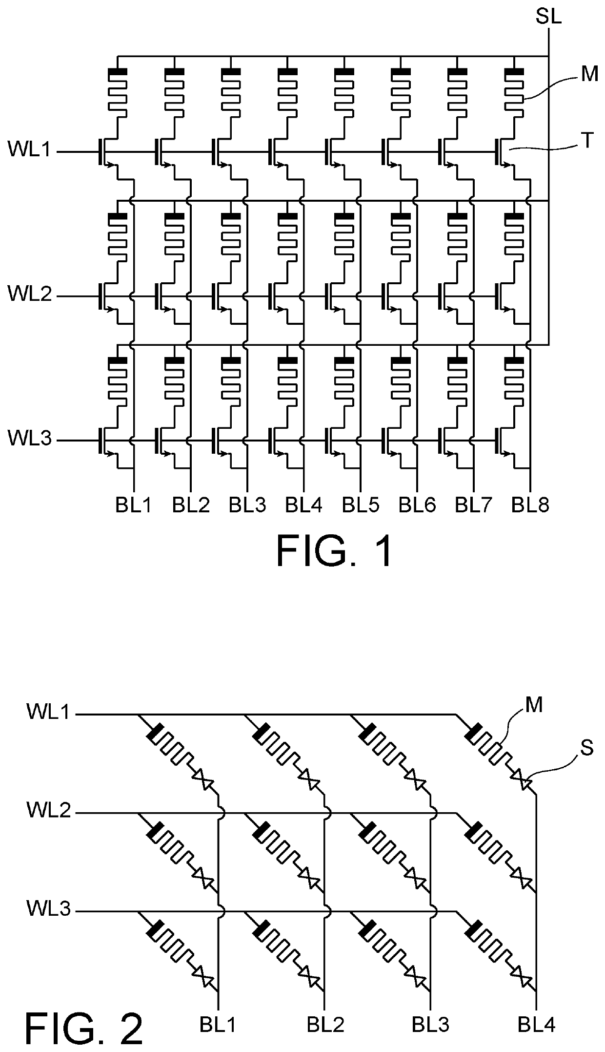
However, the presence of a transistor per synapse limits the density of such a synaptic array.
A certain number of constraints weigh on the effective implementation of such a network of artificial neurons.
For example, while the organisation of the synaptic array has advantages (parallelisation of the calculations, density, sharing of the drivers), it has limitations.
However, in certain cases, this “all-to-all” connection can lead to a principally null synaptic matrix and thus to a low energy efficiency.
This organisation also requires having to finely process the zero weights or risk having a network composed mainly of parasitic synapses, making the analogue integration of the synaptic weights even more complex.
Such a phenomenon is problematic.
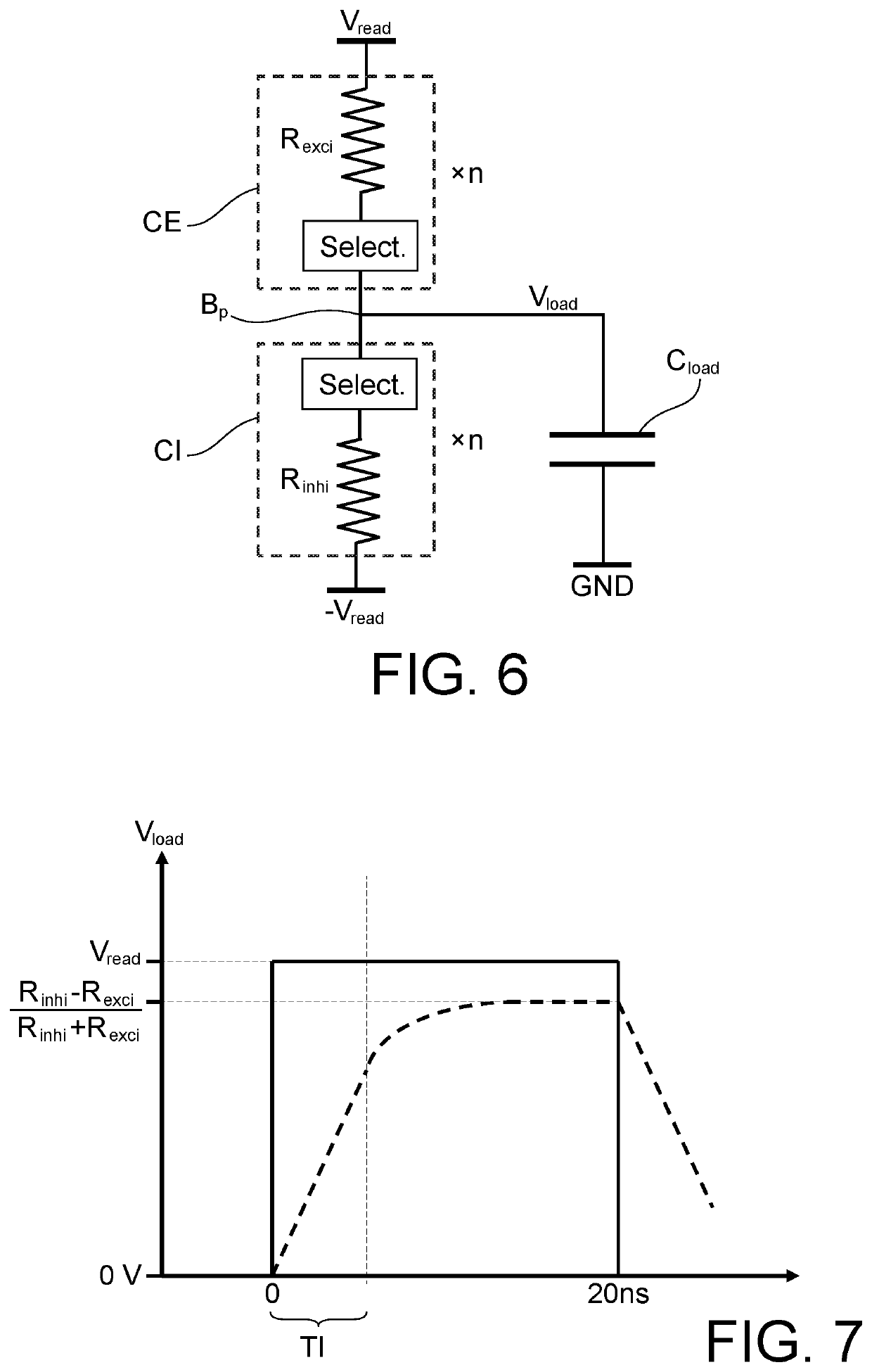
The reading of an OxRAM presents a difficulty, that of parasitic writing by modifying little by little the value of the resistance over successive readings.
The smallness of this voltage greatly complicates the implementation of integrative analogue reading of these memories.
However, since Vmem is an analogue calculation element and thus subjected in particular to issues of noise, technological variations, capacitive coupling, its voltage range cannot be reduced to a value as low as 100 mV without greatly increasing the sources of calculation errors.
Moreover, it is noted that RRAM devices often have a low range of resistance (with low values of approximately one kΩ) and that time constants of the pair Rsyn-Cmem of approximately one nanosecond or even less may be encountered.
However, it is not easy to generate read pulses of less than Ins, unless a specific circuit is used.
However, the shorter this pulse, the less it is “clean” at the end of the line.
Finally, such a pulse has difficulty propagating in active analogue circuits tasked with integrating the read current without being faced with issues of bandwidth and / or distortion.

Method used


Image

  • Artificial neuron for neuromorphic chip with resistive synapses
  • Artificial neuron for neuromorphic chip with resistive synapses
  • Artificial neuron for neuromorphic chip with resistive synapses

Examples


Embodiment Construction

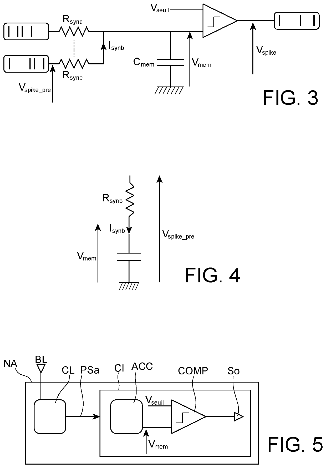
[0041]In reference to FIG. 5, the invention relates to an artificial neuron NA for a neuromorphic chip comprising a synapse with resistive memory representative of a synaptic weight.

[0042]The synapse has a terminal for activation of the synapse and a terminal for propagation of a synaptic signal. In the presence of a presynaptic activation applied onto the activation terminal, the propagation terminal propagates a synaptic signal representative of the value of the resistive memory (i.e. the synaptic weight) in the direction of the artificial neuron NA via a bit line BL.

[0043]The artificial neuron comprises an integration circuit CI that comprises an accumulator of synaptic weights ACC at the terminals of which a membrane voltage Vmem is established and a comparator COMP configured to emit a postsynaptic pulse SO if a threshold Vseuil is exceeded by the membrane voltage Vmem.

[0044]The invention proposes decoupling the reading of the synaptic weight from its integration by avoiding di...


PUM


Abstract

An artificial neuron for a neuromorphic chip comprises a synapse with resistive memory representative of a synaptic weight. The artificial neuron comprises a read circuit, an integration circuit and a logic circuit interposed between the read circuit and the integration circuit. The read circuit is configured to impose on the synapse a read voltage independent of the membrane voltage and to provide an analogue value representative of the synaptic weight. The logic circuit is configured to generate from the analogue value a pulse having a duration. The integration circuit comprises an accumulator of synaptic weights at the terminals of which a membrane voltage is established and a comparator configured to emit a postsynaptic pulse if a threshold is exceeded by the membrane voltage. Moreover, it comprises a source of current controlled by the pulse to inject a current into the accumulator of synaptic weights during this duration.

Description

TECHNICAL FIELD[0001]The field of the invention is that of neuromorphic chips with networks of artificial neurons using synapses with resistive memory.PRIOR ART[0002]A nerve cell, or neuron, can be decomposed into several parts:[0003]The dendrites which are the inputs of the neuron through which it receives excitation or inhibition signals;[0004]The body of the neuron which is the location of ionic exchanges through the cell membrane;[0005]The axon, a long extension of the cell body, which is the only output of the body.[0006]According to the excitation or inhibition signals received at the dendrites, ions transit through the cell membrane. The imbalance of charges between the inside and the outside of the cell induces a voltage difference on either side of the membrane. This is called membrane voltage at the terminals of a membrane capacitance. When this membrane voltage exceeds a certain level, that is to say when the cell is sufficiently excited, the neuron experiences an abrupt ...

Claims


Application Information

Patent Timeline
Patent Type & Authority Applications(United States)
IPC IPC(8): G06N3/063G11C13/00G11C11/54G11C11/34
CPCG11C13/004G06N3/0635G11C11/34G11C11/54G06N3/049G06N3/065G11C13/0002
Inventor RUMMENS, FRANÇOISVALENTIAN, ALEXANDRE
Owner COMMISSARIAT A LENERGIE ATOMIQUE ET AUX ENERGIES ALTERNATIVES
Learn More