Array substrate, display panel and display device

a display panel and substrate technology, applied in the field of display devices, can solve the problems of insufficient design of goa storage capacitors, excessive plane area occupied by the 1st metal layer and the 2nd metal layer, etc., and achieve the effect of increasing the capacitance of storage capacitors

Inactive Publication Date: 2020-05-14
HKC CORP LTD +1
View PDF0 Cites 0 Cited by
  • Summary
  • Abstract
  • Description
  • Claims
  • Application Information

AI Technical Summary

Benefits of technology

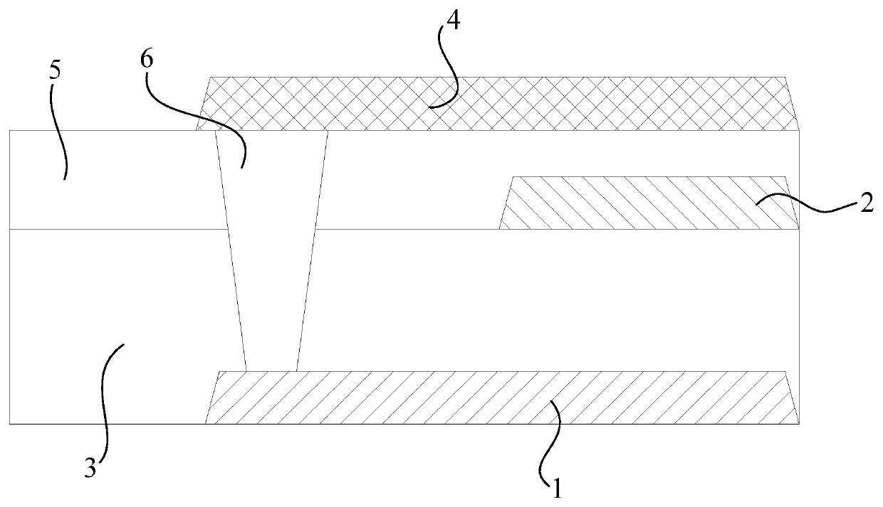
[0044]In the technical solution of this application, an electrode layer is disposed at one side where a 2nd metal layer is far away from a 1st metal layer, and an insulation layer (its thickness is smaller than that of dielectric layer) is disposed at the 2nd metal layer and the electrode layer; the electrode layer is disposed in a manner that it is electrically connected with the 1st metal layer and at least partly overlaps with the 2nd metal layer; thereby, a 1st storage capacitor of gate drive circuit is formed between the electrode layer and the 2nd metal layer; compared with the way of using the 1st metal layer and the 2nd metal layer to form storage capacitor in exemplary technology, the thickness of the insulation layer in this embodiment is smaller than that of the dielectric layer between the 1st metal layer and the 2nd metal layer, thus helping to increase the capacitance of the storage capacitor; In other words, when equivalent capacitance is kept, the plane area of the storage capacitor of this embodiment is smaller, thus reducing the plane area outside display zone of liquid crystal display device occupied by storage capacitor and helping to realize narrow frame of liquid crystal display device.

Problems solved by technology

As is known from the formula of storage capacitor ‘Holding C=ε0εrA / d’, the distance d between the 1st metal layer and the 2nd metal layer (i.e., the thickness of dielectric layer) is relatively large so that a relatively large capacity of storage capacitor can be obtained only by increasing the plane area A of the 1st metal layer and the 2nd metal layer as much as possible; however, the excessive plane area occupied by the 1st metal layer and the 2nd metal layer will conflict with the demand for narrow frame of liquid crystal display products.
In conclusion, a proper GOA storage capacitor design has not been found yet in response to high resolution and narrow frame required for liquid crystal display products.

Method used


Image

  • Array substrate, display panel and display device

Examples


Embodiment Construction

[0049]The technical solutions in the embodiments of the present application will be clearly and completely described hereafter in reference to the drawings in the embodiments of the present application. It is apparent that the described embodiments are merely a part of embodiments rather than all the embodiments of the present application. All the other embodiments obtained by the artisans concerned on the basis of the embodiments in the present application without creative efforts fall within the scope of claims of the present application.

[0050]It is to be understood that, all of the directional instructions in the exemplary embodiments of the present disclosure (such as top, down, left, right, front, back) can only be used for explaining relative position relations, moving condition of the elements under a special form (referring to the FIGURE), and so on, if the special form changes, the directional instructions changes accordingly.

[0051]In addition, the descriptions, such as the...


PUM

PropertyMeasurementUnit
thicknessaaaaaaaaaa
thicknessaaaaaaaaaa
areaaaaaaaaaaa

Abstract

This application discloses an array substrate, a display panel and a display device; a first storage capacitor is formed in a small spacing between a 2nd metal layer and an electrode layer of the array substrate.

Description

CROSS REFERENCE TO RELATED APPLICATIONS[0001]The present application is a Continuation Application of PCT Application No. PCT / CN2018 / 122110 filed on Dec. 19, 2018, which claims the benefit of Chinese Patent Application No. 201821840986.3 filed on Nov. 8, 2018. All the above are hereby incorporated by reference.FIELD OF THE DISCLOSURE[0002]This application relates to the field of display device, and particularly, to an array substrate, a display panel and a display device.BACKGROUND OF THE DISCLOSURE[0003]The description here only provides the background information on this application, and it does not necessarily constitute the existing technology. According to drive design, the process architecture of display screen can be divided into system on chip (SOC) and gate driver on array (GOA). However, as an important technology of panel design, GOA uses the method of array exposure and development to form gate drive on glass and generate logic circuit to drive gate signal line, i.e., ga...

Claims


Application Information

Patent Timeline
Patent Type & Authority Applications(United States)
IPC IPC(8): H01L27/12
CPCH01L27/1255G02F1/136213H01L27/124
Inventor LIN, PEIXIN
Owner HKC CORP LTD
Why Eureka
Try Eureka