Semiconductor Strucure with Partially Embedded Insulation Region

a technology of semi-inserting and insulation region, which is applied in the direction of semi-inserting devices, basic electric elements, electrical apparatus, etc., can solve the problems of region structure that are not possible or feasible to obtain, and achieve the effect of simplifying the design and fabrication of mixed signal i

Active Publication Date: 2020-02-20
STMICROELECTRONICS SRL
View PDF9 Cites 0 Cited by
  • Summary
  • Abstract
  • Description
  • Claims
  • Application Information

AI Technical Summary

Benefits of technology

[0007]Such unique shapes or profiles of oxide regions may be used in semiconductor devices to reduce the intrinsic parasitic N—P—N heterojunctions and o achieve local isolation of a single device or a circuit unit from the rest of the circuitry. Such local dielectric isolat...

Problems solved by technology

As such, techniques of the present disclosure can achieve unique oxide region ...

Method used


Image

  • Semiconductor Strucure with Partially Embedded Insulation Region
  • Semiconductor Strucure with Partially Embedded Insulation Region
  • Semiconductor Strucure with Partially Embedded Insulation Region

Examples


Embodiment Construction

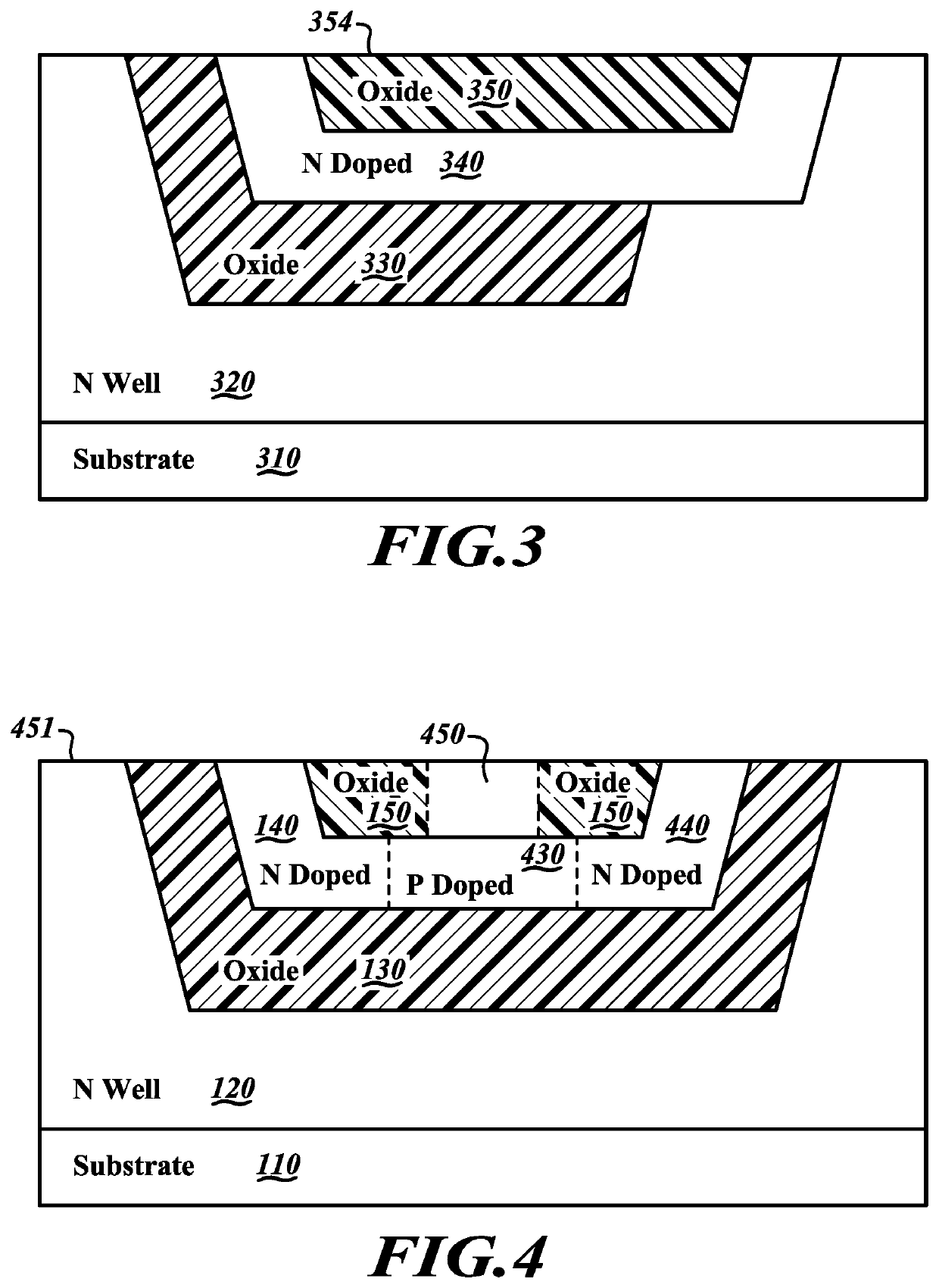
[0019]Each of the features and teachings disclosed herein may be utilized separately or in conjunction with other features and disclosure to provide methods for achieving local oxidation from porous silicon and for obtaining various distinctive structures that are enabled by the methods. Representative examples utilizing many of these additional features and teachings, both separately and in combination, are described in further detail with reference to the attached figures. This detailed description is intended to teach a person of skill in the art further details for practicing aspects of the present disclosure, and is not intended to limit the scope of the claims. Therefore, combinations of features disclosed in the detailed description may not be necessary to practice the teachings in the broadest sense, and are instead disclosed merely to describe particularly representative examples of the present disclosure.

[0020]Unless the context requires otherwise, throughout the specifica...


PUM


Abstract

A technique to make silicon oxide regions from porous silicon and related semiconductor structures are disclosed. The porous silicon is made in situ by anodizing P doped silicon regions. Thus, the shape and profile of the oxide regions may be controlled by controlling the shape and profile of the P doped silicon regions.

Description

BACKGROUNDTechnical Field[0001]The present disclosure relates to semiconductor devices and technologies with various oxide layers for insulation.Description of the Related Art[0002]Mixed signal integrated circuits (“IC”) combine analog circuitry with digital circuitry. Devices of digital circuitry (digital devices) are subject to low electric current and voltages, and function as switches to achieve logical or arithmetic functions, among other things. Devices of analog circuitry (analog devices) may be exposed directly to high voltage scenarios of input voltage or current signals, power regulation and amplification, and power sensing.[0003]Merged bipolar-CMOS-DMOS processes (“BCD”) have been used to fabricate mixed signal ICs. Due to the differences in the signal or working regimens of the bipolar devices, CMOS devices and DMOS, such as BCD structures, include complex processes to form various insulation regions to isolate the various devices. Generally a BCD device includes shallow...

Claims


Application Information

Patent Timeline
IPC IPC(8): H01L21/762H01L21/306H01L21/02H01L29/06
CPCH01L21/76213H01L29/0649H01L21/306H01L21/02164H01L21/02238H01L21/02203H01L29/7824H01L21/76245
Inventor MARIANI, SIMONE DARIOTOIA, FABRIZIO FAUSTO RENZOSAMBI, MARCOPATTI, DAVIDE GIUSEPPEMORELLI, MARCOBARILLARO, GIUSEPPE
Owner STMICROELECTRONICS SRL
Why Eureka
Try Eureka