Semiconductor device
- Summary
- Abstract
- Description
- Claims
- Application Information
AI Technical Summary
Benefits of technology
Problems solved by technology
Method used
Image

Examples
first embodiment
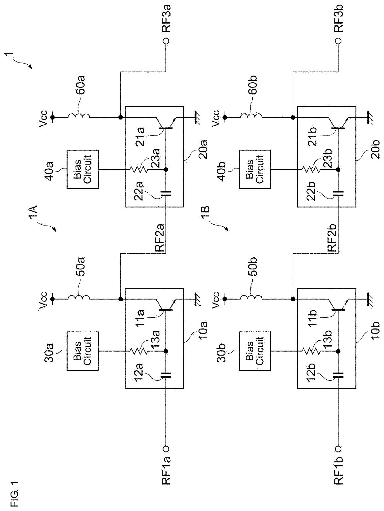
[0026]FIG. 1 is a circuit diagram of a power amplifier circuit 1 included in a semiconductor device according to the present disclosure. As illustrated in FIG. 1, the power amplifier circuit 1 is mounted in, for example, a mobile communication apparatus such as a cellular phone, and amplifies the power of a radio frequency (RF) signal to be transmitted to a base station. The frequency of an RF signal to be amplified is, for example, about several to tens of GHz.
[0027]The power amplifier circuit 1 includes two paths, that is, a path 1A and a path 1B. The paths 1A and 1B are selectively used in accordance with, for example, a difference in the communication standard or frequency band of the RF signal to be amplified. Here, it is assumed that the path 1A is supplied with an input signal RF1a in a first frequency band and that the path 1B is supplied with an input signal RF1b in a second frequency band.
[0028]The paths 1A and 1B include amplifiers 10a and 10b in a first stage (drive stag...
third embodiment
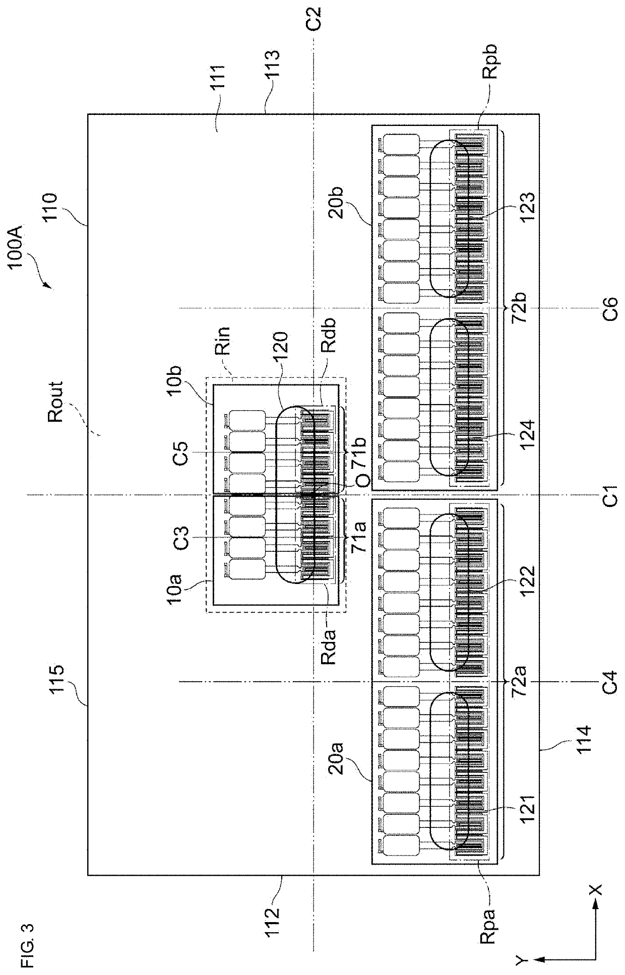
[0068]FIG. 6 is a plan view of a semiconductor device 100C according to the present disclosure. As illustrated in FIG. 6, the semiconductor device 100C is different from the semiconductor device 100A illustrated in FIG. 3 in the orientations of the unit cells of the amplifiers 20a and 20b in the second stage of each of the paths 1A and 1B and in the shapes and the number of bumps. Specifically, the semiconductor device 100C includes bumps 126 to 133 instead of the bumps 121 to 124.
[0069]In the present embodiment, in the amplifier 20a in the second stage of the path 1A, the sixteen unit cells 72a are aligned in units of four unit cells in the X-axis direction. The four unit cells aligned in the X-axis direction are regarded as one line, and four lines are aligned in the Y-axis direction. In the present embodiment, the center line C4 along the Y axis of the region Rpa is a boundary line that splits the four unit cells 72a into two groups each including two unit cells, and the center l...
fourth embodiment
[0071]FIG. 7 is a plan view of a semiconductor device 100D according to the present disclosure. As illustrated in FIG. 7, the semiconductor device 100D is different from the semiconductor device 100A illustrated in FIG. 3 in the arrangement of the amplifier 20b in the second stage of the path 1B and in the arrangement of bumps.
[0072]In the present embodiment, the sixteen unit cells 72b included in the amplifier 20b in the second stage of the path 1B are aligned in one line in the Y-axis direction between the center line C1 of the semiconductor substrate 110 and the side 113 in the peripheral region Rout. The center line in the X-axis direction of the region Rpb in which the sixteen unit transistors are disposed overlaps the center line C2 of the semiconductor substrate 110. The unit cells 71b included in the amplifier 10b in the first stage of the path 1B are aligned near the center line C2. The bumps 123 and 124 are arranged on the unit cells 72b in accordance with the alignment of...
PUM
 Abstract
Description
Claims
Application Information
 - R&D
- Intellectual Property
- Life Sciences
- Materials
- Tech Scout
- Unparalleled Data Quality
- Higher Quality Content
- 60% Fewer Hallucinations
Browse by: Latest US Patents, China's latest patents, Technical Efficacy Thesaurus, Application Domain, Technology Topic, Popular Technical Reports.
© 2025 PatSnap. All rights reserved.Legal|Privacy policy|Modern Slavery Act Transparency Statement|Sitemap|About US| Contact US: help@patsnap.com