SiC WAFER AND MANUFACTURING METHOD OF SiC WAFER

Pending Publication Date: 2020-01-16
DENSO CORP +1
View PDF2 Cites 0 Cited by
  • Summary
  • Abstract
  • Description
  • Claims
  • Application Information

AI Technical Summary

Benefits of technology

The present invention relates to a method for manufacturing a SiC wafer that allows for the identification of defects after device construction in a non-destructive manner. This enables the identification of any defects that may cause failure of a semiconductor device, which can improve the efficiency and accuracy of the manufacturing process.

Problems solved by technology

At this time, when there is a defect in a SiC wafer which is a substrate forming a semiconductor device, abnormality may be incurred in the semiconductor device (for example, PTL 1 and the like).
On the other hand, various defects are present in the SiC epitaxial wafer.
That is, depending on the kind of defect, defects having no or little influence on semiconductor devices are present.
For example, it is known that threading dislocations and the like become a cause of failure of a semiconductor device, but it is not precisely known which defect mode can particularly become a killer defect, among the threading dislocations.

Method used


Image

  • SiC WAFER AND MANUFACTURING METHOD OF SiC WAFER
  • SiC WAFER AND MANUFACTURING METHOD OF SiC WAFER

Examples


Embodiment Construction

[0021]Hereinafter, an embodiment will be described in detail with reference to the drawings as appropriate. In the drawings used in the following description, in order to facilitate understanding of the features of the present invention, there are cases where characteristic portions are enlarged for convenience, and the dimensional ratio and the like of each constituent element may be different from reality. In addition, the materials, dimensions, and the like shown in the following description are merely examples, and the present invention is not limited thereto and can be embodied in appropriately modified manners in a range that does not change the gist thereof.

[0022](SiC Wafer)

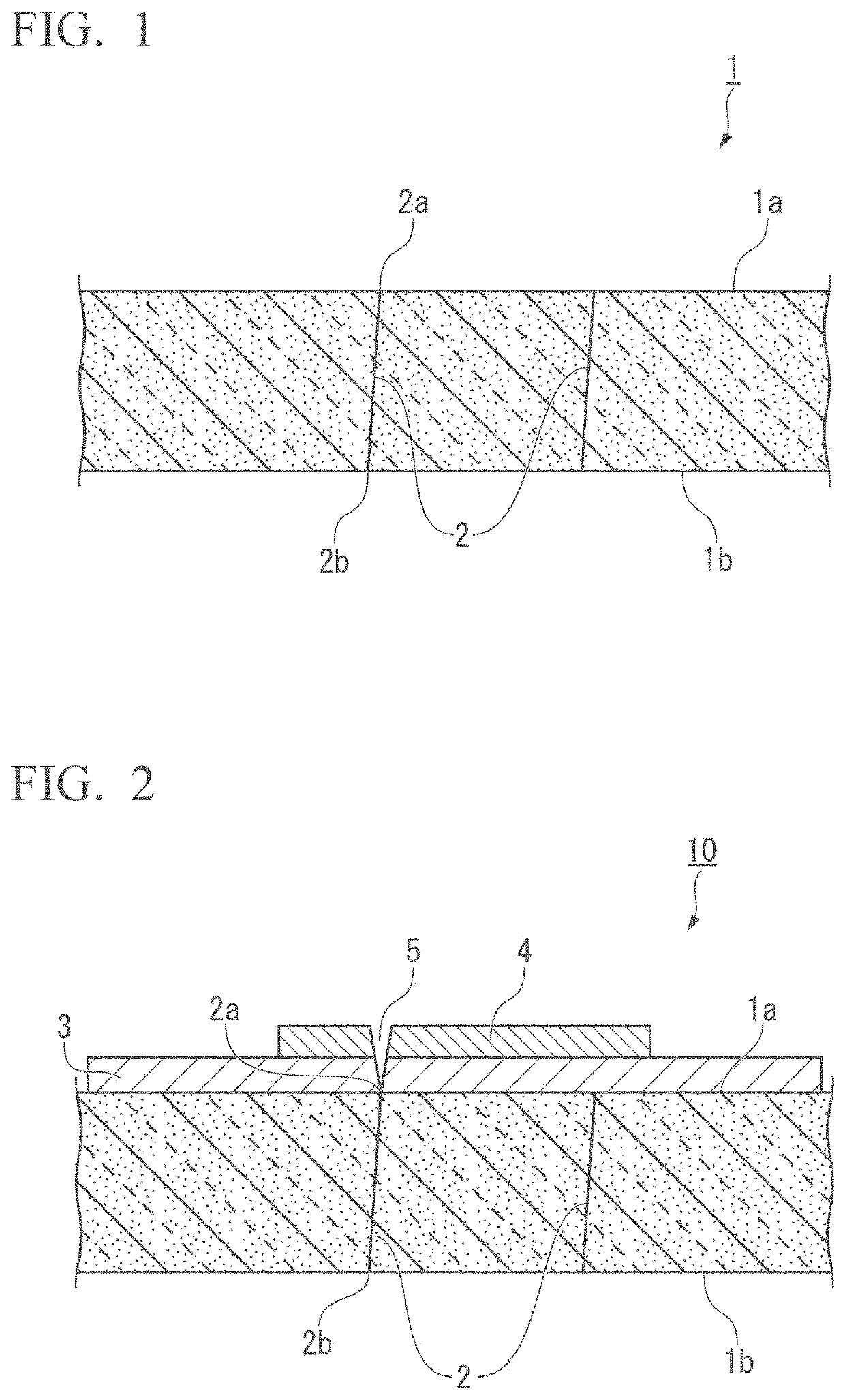
[0023]FIG. 1 is a schematic sectional view of a SiC wafer according to an embodiment of the present invention. A SiC wafer 1 illustrated in FIG. 1 has threading dislocations 2 penetrating a first surface 1a and a second surface 1b.

[0024]The SiC wafer 1 typically uses a c-plane: (0001) plane as its princip...


PUM


Abstract

In a SiC wafer, a difference between a threading dislocation density of threading dislocations exposed on a first surface and a threading dislocation density of threading dislocations exposed on a second surface is 10% or less of the threading dislocation density of the surface with a higher threading dislocation density among the first surface and the second surface, and 90% or more of the threading dislocations exposed on the surface with a higher threading dislocation density among the first surface and the second surface extend to the surface with a lower threading dislocation density.

Description

TECHNICAL FIELD[0001]The present invention relates to a SiC wafer and a manufacturing method of a SiC wafer.[0002]Priority is claimed on Japanese Patent Application No. 2016-250804, filed on Dec. 26, 2016, the content of which is incorporated herein by reference.BACKGROUND ART[0003]Silicon carbide (SiC) has a dielectric breakdown field larger by one order of magnitude and a band gap three times larger than those of silicon (Si). In addition, silicon carbide (SiC) has characteristics such that the thermal conductivity is approximately three times higher than that of silicon (Si). Therefore, application of silicon carbide (SiC) to power devices, high-frequency devices, high-temperature operation devices, and the like is expected.[0004]As a semiconductor device using a SiC epitaxial wafer, a metal-oxide-semiconductor field-effect transistor (MOSFET) is known. In the MOSFET, a gate oxide film is formed on a SiC epitaxial layer by thermal oxidation or the like, and a gate electrode is fo...

Claims


Application Information

Patent Timeline
IPC IPC(8): H01L29/16C30B23/02C30B29/36
CPCC30B23/025H01L29/1608C30B29/36C30B23/06
Inventor FUJIKAWA, YOHEITAKABA, HIDETAKA
Owner DENSO CORP
Why Eureka
Try Eureka