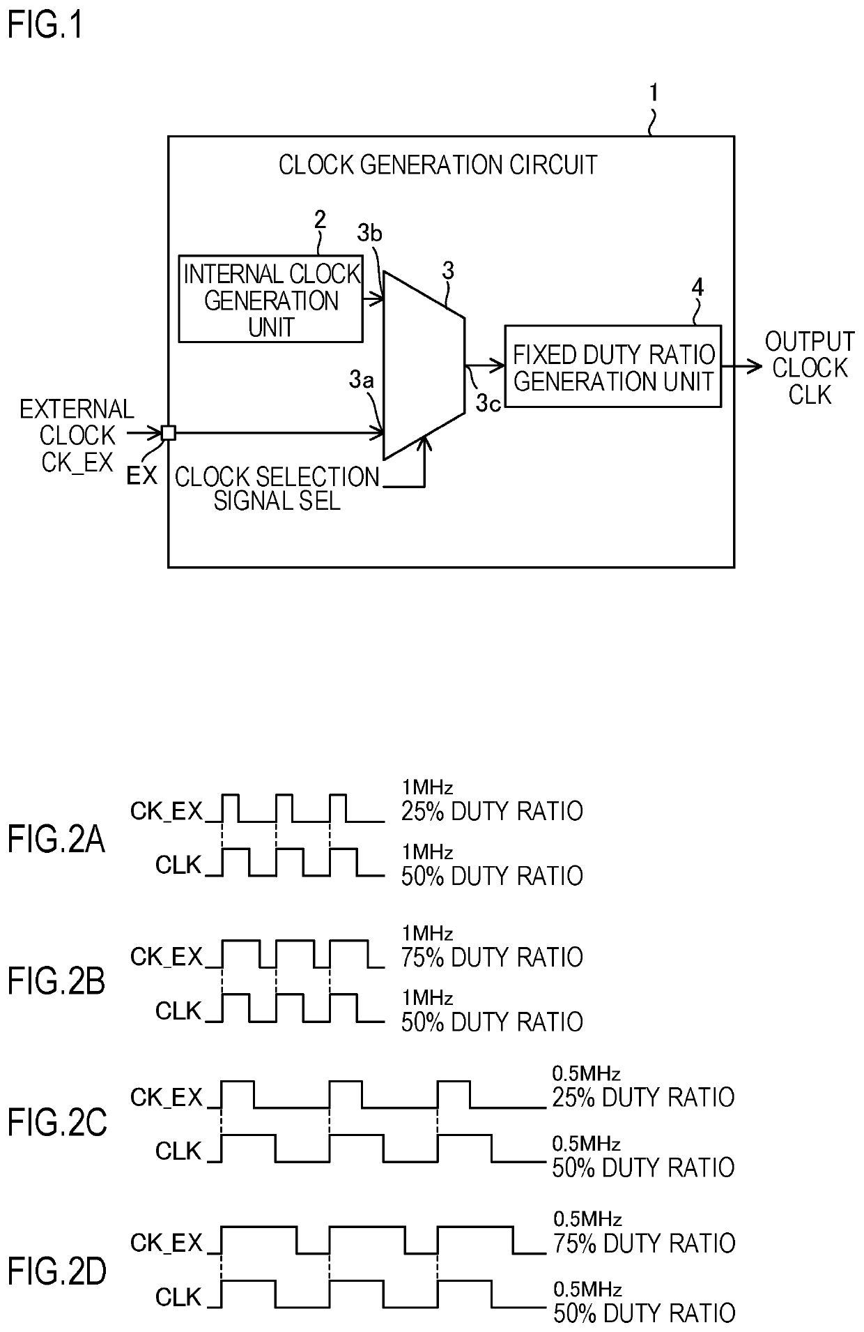
Clock generation circuit, switching power supply device, and semiconductor device
a clock generation circuit and switching power supply technology, applied in the direction of generating/distributing signals, power conversion systems, dc-dc conversion, etc., can solve the problems of large circuit scale of the pll circuit and large clock generation circui
- Summary
- Abstract
- Description
- Claims
- Application Information
AI Technical Summary
Benefits of technology
Problems solved by technology
Method used
Image

Examples
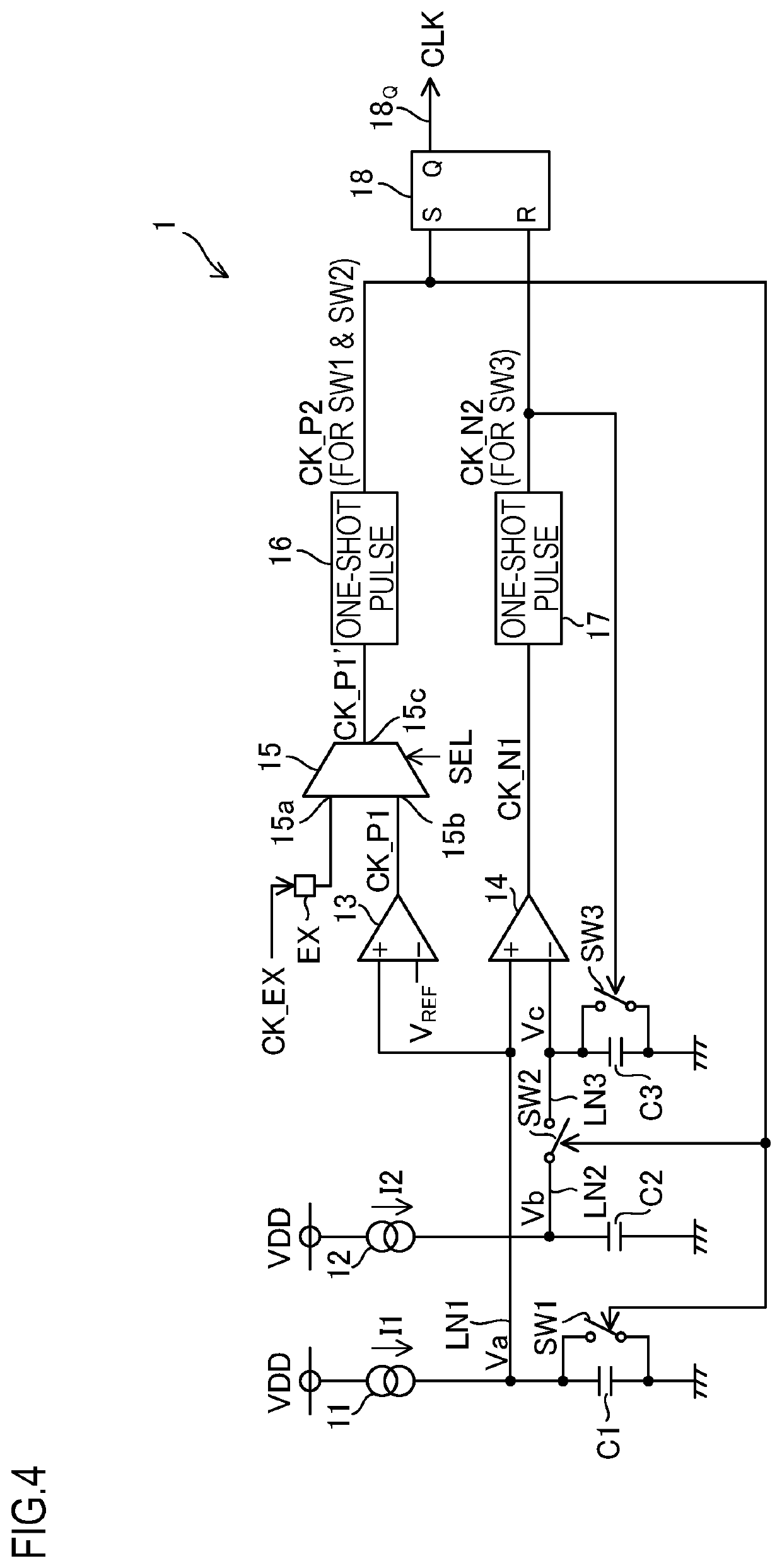
first example
[0072]A first example is described below. In the first example, as illustrated in FIG. 6, it is supposed that the external clock CK_EX is input to the input terminal EX, and that the selection signal SEL is “1”. In addition, it is supposed that capacitance values of the capacitors C1, C2, and C3 are the same, and that the value of the constant current I2 is ½ of the value of the constant current I1. In this case, the fixed duty ratio is set to 50% (the reason will be apparent from the following description).
[0073]FIG. 7 is a signal waveform diagram under supposition of the first example. A certain period of the external clock CK_EX is noted, and the up edge timing of the external clock CK_EX is regarded as a starting point, for describing the operation of the clock generation circuit 1. In FIG. 7, a solid polygonal line 510a, a broken polygonal line 510b, and a dot-dashed polygonal line 510c indicate waveforms of the voltages Va, Vb, and Vc, respectively.
[0074]At timing TA1, an up e...
second example
[0081]A second example is described. In the second example, as illustrated in FIG. 8, it is supposed that the external clock CK_EX is not input to the input terminal EX and that the selection signal SEL is “0”. In addition, it is supposed that the capacitance values of the capacitors C1, C2, and C3 are the same, and that the value of the constant current I2 is ½ of the value of the constant current I1 In this case, similarly to the first example, the fixed duty ratio is set to 50%.
[0082]FIG. 9 is a signal waveform diagram under supposition of the second example. When the external clock CK_EX is not input, the output clock CLK is generated in synchronization with the signal CK_P1 as the internal clock. An up edge occurs periodically in the signal CK_P1, and an occurrence interval of the up edges in the signal CK_P1 corresponds to the period of the internal clock. A certain period of the internal clock is noted, and the up edge timing of the internal clock is regarded as a starting po...
third example
[0090]A third example is described. In the third example, as illustrated in FIG. 10, it is supposed that the external clock CK_EX is input to the input terminal EX and that the selection signal SEL is “1”. In addition, it is supposed that the capacitance values of the capacitors C1, C2, and C3 are the same, and that the value of the constant current I2 is ⅓ of the value of the constant current I1. In this case, the fixed duty ratio is set to ⅓ (approximately 33%).
[0091]FIG. 11 is a signal waveform diagram under supposition of the third example. A certain period of the external clock CK_EX is noted, and the up edge timing of the external clock CK_EX is regarded as a starting point, for describing the operation of clock generation circuit 1. In FIG. 11, a solid polygonal line 530a, a broken polygonal line 530b, a dot-dashed polygonal line 530c indicate waveforms of the voltages Va, Vb, and Vc, respectively.
[0092]An up edge (i.e. switch from low level to high level) occurs in the exter...
PUM
 Abstract
Description
Claims
Application Information
 - R&D
- Intellectual Property
- Life Sciences
- Materials
- Tech Scout
- Unparalleled Data Quality
- Higher Quality Content
- 60% Fewer Hallucinations
Browse by: Latest US Patents, China's latest patents, Technical Efficacy Thesaurus, Application Domain, Technology Topic, Popular Technical Reports.
© 2025 PatSnap. All rights reserved.Legal|Privacy policy|Modern Slavery Act Transparency Statement|Sitemap|About US| Contact US: help@patsnap.com